Polymer Innovation Blog

Practical tips and advice for polymer, innovation and product development professionals

Polymer Innovation
  • Home
  • eBooks
    • Polymers in Electronic Packaging
    • Rheology of Thermosets eBook
    • Practical Tips for Curing Thermosets
    • Thermoset Characterization
    • Dielectric Cure Monitoring of Thermosets
    • Introduction to Biopolymers and Bioplastics
  • Videos
    • Core Curriculum: 3 Part Video Series
    • Characterization of Thermosets: 4 Part Video Series
    • Advanced Thermoset Cure Kinetics: 3 Part Video Series
    • DSC of Polymers: 5 Part Video Series
    • Thermoplastics: 5 Part Video Series
  • Services
    • Consulting
    • Polymer Expert Witness
  • Learning Center
    • White Paper
  • Why Jeff?
    • Speaker Info
  • Contact
  • Subscribe
  • Members
    • Login
    • Logout

Polymers In Electronic Packaging: Introduction to Wafer-Level Underfill

July 15, 2019 By Jeffrey Gotro 1 Comment

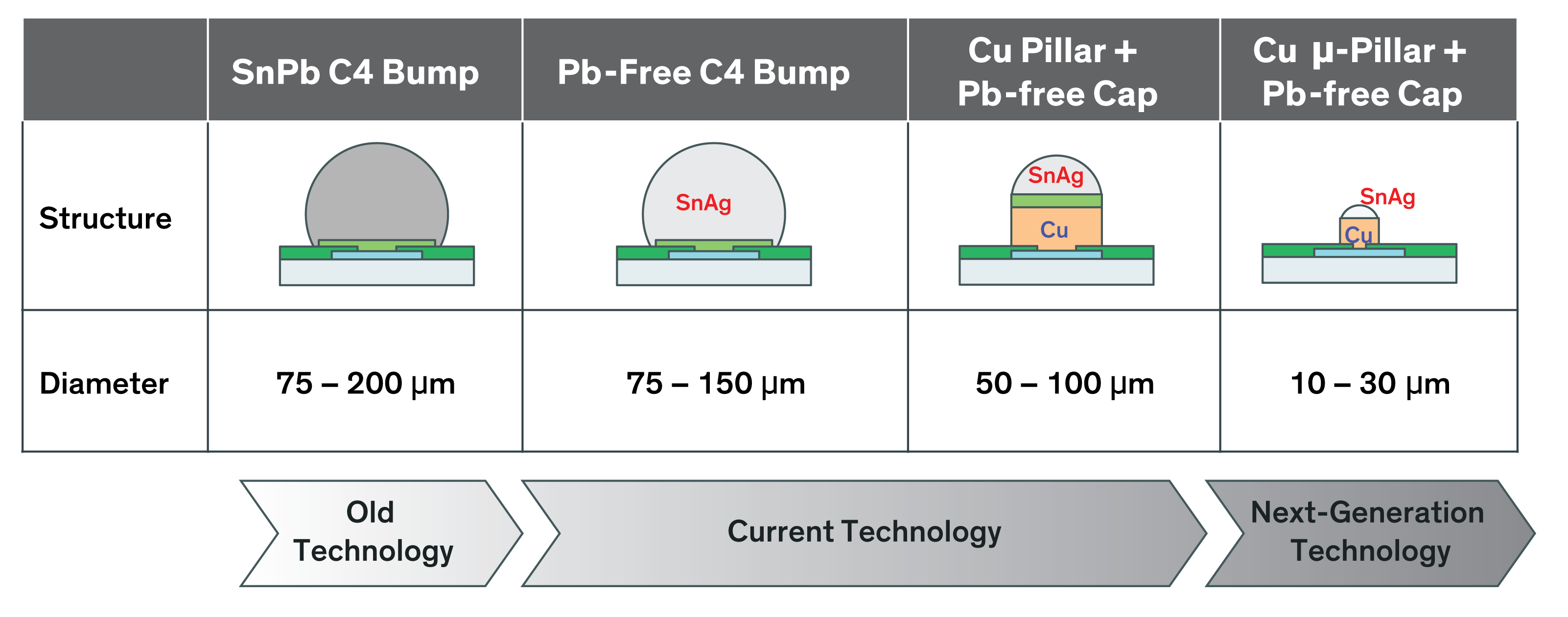
Image from DuPont Electronic Solutions [1].

A previous post described the challenges associated with the future use of capillary underfills. The technical drivers for the next generation of underfills are:

  • Bump pitch going to less than 100 microns
  • Bump diameter is moving to less than 50 microns
  • CTE of the underfill needs to be in the range of 20 ppm/°C
  • Large dies will have thousands of copper pillars to interconnect
  • Low K ILD (inner layer dielectric) in chip requires stress control and a robust pillar joining process.

Note: since the previous post, copper pillars with lead-free solder tips has replaced solder bumps as the preferred method to make chip-to-substrate interconnections.

To address the technical challenges in the list above, pre-applied underfills or wafer-applied underfills are being developed.  There are two types of pre-applied underfills:

  1. Wafer level underfills that are coated onto the wafer and B-stages
  2. Non-conductive film (NCF) that is laminated onto the wafer

The processes for each are shown in Figure 1.

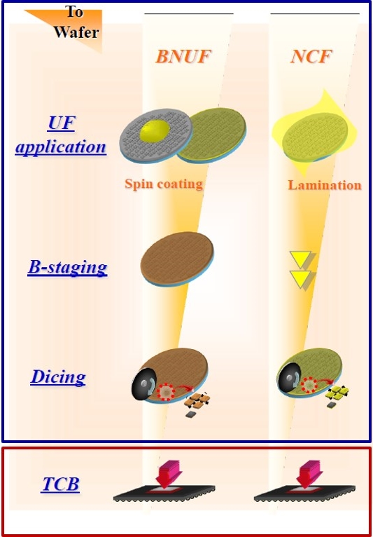
Figure 1. Wafer-level underfills using two methods: B-staged no-flow underfill (BNUF) and non-conductive film (NCF).  Image courtesy of Namics.

The process used for the B-staged no-flow underfill was presented in a previous post.

There are several material suppliers developing non-conductive film underfill such as Namics, Dow Electronic Materials and Henkel Electronic Materials. The wafer level underfill process shown in Figure 1 starts with the lamination of the non-conductive film.  In this case, the underfill film is manufactured in a separate process yielding a very uniform thickness, B-staged, highly-filled underfill film. Subsequent posts will discuss the materials available from several suppliers.  The NCF is laminated onto the top side of the wafer.

The process flow is shown Figure 2.

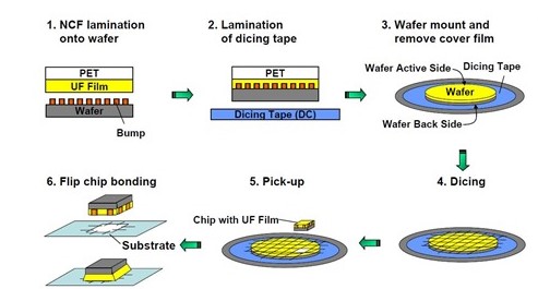
Figure 2. Non-conductive underfill (NCF) process flow

An additional challenge with the non-conductive film approach is that the film and B-staged properties have to allow:

  • Adequate flow and wetting to allow the NCF to flow over the features on the wafer front side (#1 above)
  • Good adhesion of the NCF to the wafer front side and good mechanical properties to prevent the NCF from being damaged during the dicing process (#4 above)
  • Rapid softening, flow and wetting of the substrate during thermocompression bonding (#5 above)

The thermocompression bonding process is critical to achieve both electrical joining of the thousands of copper pillars and formation of a void-free underfill with a uniform fillet around the periphery of the flip-chip.

The TC bonding process is shown in Figure 3.

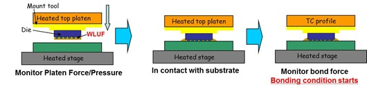
Figure 3. Thermocompression bonding process for Wafer-level underfill film (WLUF) or alternately called non-conductive film (NCF)

The interested reader may refer to a previous post on the details of the thermocompression bonding process.  Subsequent posts will discuss the various types of non-conductive films under development.

References

  1. Evolution of bumping image from DuPont Electronic Solutions Copper pillar electroplating tutorial.
Share on LinkedIn Share

Filed Under: Uncategorized

« Panel Process for Fan Out Wafer Level Packaging: Part Four, Build-Up Films for Redistribution Layers (RDL)
Polymers In Electronic Packaging: Non-Conductive Film (NCF) Underfill »

Leave a Reply

Your email address will not be published. Required fields are marked *

Polymer Innovation Blog

I’m Dr. Jeff Gotro and welcome to the Polymer Innovation Blog. Over the last 40 years I have been involved in polymer research, along with product and process development. I acquired invaluable experience working for IBM, AlliedSignal, Honeywell, Ablestik Labs (now Henkel) and in multiple consulting projects. In this blog, I (along with some guest contributors) will share our experiences, tips, and “tricks of the trade” to get more out of your innovation efforts and discuss new trends and technical advances in the polymer industry.
View Jeff Gotro, Ph.D., CMC's profile on LinkedIn

Innocentrix, LLC


Click to Visit Website

plastics expert witness
Click for More Information

Subscribe by Email

Search the Blog

Polymer Video Training

Visit our Video Store

Polymers in Electronic Packaging

polymers in electronic packaging Are you confused about what is electronic packaging? Have you ever wondered what type of polymers and polymer-based composites are used in electronics? Learn More...

Practical Tips for Curing Thermosets

practical tips for curing thermosets Have you ever had a question about the degree of cure or is your part fully cured after processing? Confused about what is gelation or how does vitrification impact thermoset curing? Learn More...

Rheology of Thermosets

rheology of thermosets Have you ever had a question about measuring the rheological properties of thermosets Didn’t know what is the right experimental approach to get the right rheological information? Learn More...

Dielectric Cure Monitoring of Thermosets

Dielectric Cure Monitoring of Thermosets Do you have a need for an in-situ cure monitor for a thermoset process but don’t know where to start? Are you confused about the terminology used in dielectric spectroscopy? Learn More...

Introduction to Biopolymers and Bioplastics

Introduction to Biopolymers and Bioplastics Would you like to know how sustainable are bio-based polymers? Or what is the market size and growth rate for bioplastics? Or have questions about the biomass supply chain? Learn More...

Thermoset Characterization

Thermoset Characterization Have you ever had a question about how to measure a physical property of a thermoset? Confused about what is gelation or how does vitrification impact thermoset curing profiles? Or wondered how to measure the glass transition temperature of an epoxy or polyester composite? Learn More...

Amazon.com Bookshelf

Robert's Rules of Innovation Thermal Analysis of Polymers Order

Copyright © 2025 Innocentrix, LLC · All Rights Reserved