 In the last post we outlined the technical drivers for underfills and showed examples of the first type of non-capillary underfill called No-flow underfill (NUF) and introduced the concept of thermocompression (TC) bonding as the process that yielded the best results in the past.
Wafer level underfills are becoming more popular and have two embodiments:
- Non-conductive film (NCF) that is laminated onto the wafer
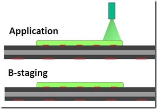
- Wafer level underfills that are coated using several methods and B-staged
Both of these methods required development of new highly filled underfills but with the added challenge of also developing new ways to apply to the wafer. The chemistry needed to be tailored to allow partial curing (B-staging) for:
- Increase the molecular weight and modulus to provide integrity during dicing (good edges along the saw streets with no chipping or cracking)
- Controlled flow during thermocompression bonding
- 6 month shelf life (coat – store – dice – TC bonding)
Why wafer level underfill?
- Flux and flux cleaning process eliminated
- Fluxing agents are included in the underfill formulations
- Reflow occurs with underfill surrounding the bump metallurgy
- Supports the bump during reflow (less inner layer dielectric (ILD) cracking
- Curing and bump joining occur simultaneously
- Pre-applied underfill (both NCF and coated/B-staged) protects the bumped die from mechanical damage
- Consolidates multiple operations
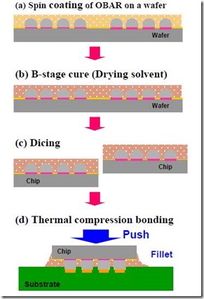
IBM and Sumitomo Bakelite published a paper at the Electronics Components and Technology Conference (ECTC) in 2011 showing the following wafer level process:
The above process uses spin coating to apply the underfill over the bumps in a process called OBAR, Over Bump Applied Resin. After spin coating, the wafer level underfill is partially cured (B-staged) to allow successful dicing in the next step. The final step in the process is thermocompression (TC) bonding.
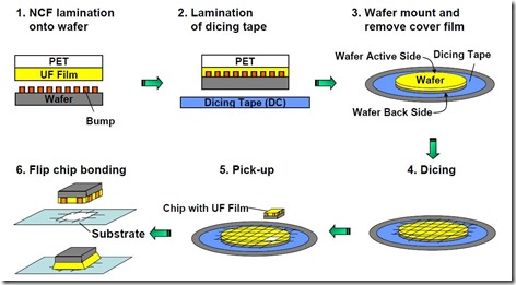
Several material suppliers are developing non-conductive film underfill. In this case, the underfill film is manufactured in a separate process yielding a very uniform thickness, B-staged, highly-filled underfill film. The film is then laminated onto the top side of the wafer. The process flow is given in the next figure:
An additional challenge with the non-conductive film approach is that the film and B-staged properties have to allow:
- Adequate flow and wetting to allow the NCF to flow over the features on the wafer front side (#1 above)
- Good adhesion of the NCF to the wafer front side and good mechanical properties to prevent the NCF from being damaged during the dicing process (#4 above)
- Rapid softening, flow and wetting of the substrate during thermocompression bonding (#5 above)
For both the wafer level applied underfill (OBAR and exposed bumps) and the NCF, the thermocompression bonding process is critical. The TC bonding process is shown in the next figure:
In the next post we will discuss in more detail the thermocompression bonding process.


Leave a Reply