
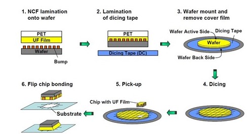
Figure 1. Non-conductive Film process flow
The last post described the technical challenges when using capillary underfills. Pre-applied underfills or wafer-applied underfills are being developed. There are three types of pre-applied underfills:
- Wafer level underfills that are coated onto the wafer and B-staged
- Non-conductive paste (NCP) that is dispensed onto the substrate prior to thermocompression bonding
- Non-conductive film (NCF) that is laminated onto the wafer, diced, and the chip with the NCF applied is joined using thermocompression bonding
This post will focus on non-conductive film. The technical requirements for NCF include:
- Good flow around copper pillars during lamination onto the bumped wafer
- Good wetting and adhesion of the NCF to the wafer front side
- The laminated NCF is robust enough to prevent being damaged during the dicing process
- Transparency to allow the fiducials to be imaged during thermocompression bonding
- Rapid softening, flow and wetting of the substrate during thermocompression bonding
- Fast curing during thermocompression bonding
- High glass transistion temperature (Tg) and low coefficient of thermal expansion (CTE) for thermal cycle reliability
There are several material suppliers developing non-conductive film underfill such as Namics, Dow Electronic Materials and Henkel Electronic Materials. The wafer level underfill process shown in Figure 1 starts with the lamination of the non-conductive film. In this case, the underfill film is manufactured in a separate process yielding a very uniform thickness, B-staged, highly-filled underfill film. The underfill material is coated onto a PET carrier and then covered with a protective release film. The shelf-life of the coated NCF should be at least 6 months. The film thickness is governed by the copper pillar height, the bottom pad thickness, and the solder tip collapse during bonding.
Figure 2 shows the NCF coating process for a Dow Electronic Materials NCF.

Figure 2. NCF coating and lamination process [from reference 1]
The Dow NCF thickness control is ± 0.5 µm across a 330 mm wide roll. The Dow literature describes two scenarios for covering the copper pillars. In the top process flow in Figure 2, the lamination process leaves the tip of the pillar exposed. In another process flow, the NCF underfill covers the entire pillar as shown in the image on the lower right side in Figure 2. If the pillars are covered, the transparency of the underfill film becomes a key factor.
During thermocompression bonding, the TCB imaging cameras will scan the substrate and the die to locate fiducials in order to make sure there will be proper alignment of the pillar and the pad. Thus, the underfill film must be transparent. With the requirement of low CTE, the underfill films are typically highly-filled with well-controlled silica particles. In order to achieve transparency, the filler particle size must be small. In Figure 3, an example of a non-transparent and transparent NCF is shown.
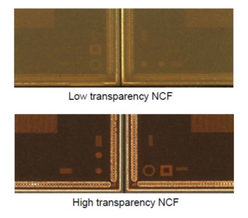
Figure 3. Low and High Transparency NCF examples [from Henkel, reference 2]
The underfill film in the lower photograph has high transparency allowing imaging of the fiducials during TDB. The lower transparency underfill film in the upper portion in Figure 3 would cause errors in registration during the TCB process. Material suppliers are skilled at selecting the right particle sizes and particle size distributions (i.e. multi-modal particle size distributions) to achieve the desired CTE and transparency. The exact details of the particle sizes and surface treatments are typically proprietary, i.e. the formulators “secret sauce!”
The next post will discuss the thermocompression bonding process for NCF.
References
- M. Calvert, MEPTEC presentation, April 9. 2014
- Jie Bai, et. al., Enabling Reliability of 3D TSV Advanced Packages with Non-Conductive, Pre-Applied Underfill Film Materials, International Wafer Level Packaging Conference (IWLPC), October 22, 2018
Leave a Reply