Polymer Innovation Blog

Practical tips and advice for polymer, innovation and product development professionals

Polymer Innovation
  • Home
  • eBooks
    • Polymers in Electronic Packaging
    • Rheology of Thermosets eBook
    • Practical Tips for Curing Thermosets
    • Thermoset Characterization
    • Dielectric Cure Monitoring of Thermosets
    • Introduction to Biopolymers and Bioplastics
  • Videos
    • Core Curriculum: 3 Part Video Series
    • Characterization of Thermosets: 4 Part Video Series
    • Advanced Thermoset Cure Kinetics: 3 Part Video Series
    • DSC of Polymers: 5 Part Video Series
    • Thermoplastics: 5 Part Video Series
  • Services
    • Consulting
    • Polymer Expert Witness
  • Learning Center
    • White Paper
  • Why Jeff?
    • Speaker Info
  • Contact
  • Subscribe
  • Members
    • Login
    • Logout

Panel Process for Fan Out Wafer Level Packaging: Part Three, Film Epoxy Mold Compounds

June 24, 2019 By Jeffrey Gotro 1 Comment

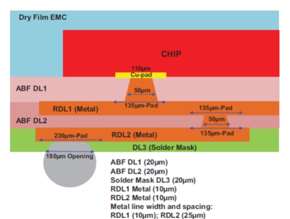
Figure 1. Cross-section from the Unimicron process from reference [1].

The last post discussed the dry film EMC using a printed circuit board vacuum lamination approach.  The panel size was 508 mm x 508 mm [1].  Panel level processing will ultimately result in lower cost per unit.

What will be some of the major technical challenges?  The epoxy molding compound (EMC) encapsulation process will need to be optimized for a panel format.  Liquid EMC will be difficult to process in the panel format since new tools will be required and achieving uniform thickness across a large panel will be difficult. In response to the need for a panel level EMC, several EMC suppliers have developed EMC in sheet form.   As shown in Figure 2, Hitachi Chemical has developed an embedded insulation resin for chip sealing called EBIS.

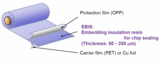
Figure 2. Film-based epoxy mold compound for FOWLP (source: Hitachi Chemical)

In this form, the highly-filled epoxy base resin is coated onto a carrier in thicknesses ranging from 50 – 250 µ).  The EMC film is used in a vacuum lamination process to encapsulate the chips on the re-constituted wafer or panel.  Ajinomoto Fine-Techno has also developed two types of epoxy mold compounds; liquid EMC (called the MI Series) for wafer level fan-out packages and a film EMC (called the LE Series) for the panel level fan-out process.

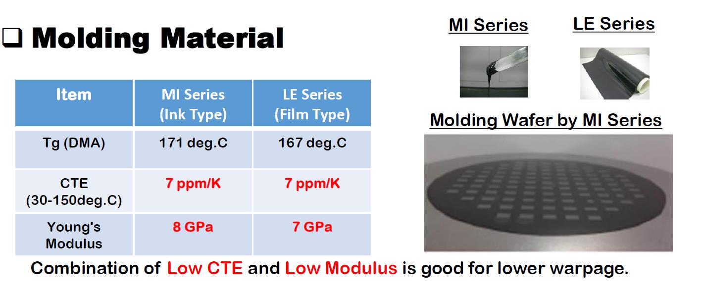
Figure 3.  Two types of epoxy molding compounds for fan-out packaging (source: Ajinomoto Fine-Techno LTD)

From the table in Figure 3, the glass transition temperature (Tg) is in the range typical of cured EMC.  One property to note is that for the FOWLP process, the coefficient of thermal expansion (CTE) needs to be very low and is usually matched to the CTE of the carrier.  Note that the CTE reported in Figure 3, is identified as the CTE below the glass transition temperature.  I also like the details provided which indicate the Tg was measured using dynamic mechanical analysis (DMA) and the CTE reported was over the temperature range of 30-150°C. The major driver for lowering the CTE and modulus is to reduce warpage after EMC processing either in the wafer or panel process.

In the last post, data was presented for a new film-based epoxy mold compound used in the Unimicron process.  For ease of comparison, the data is presented in Table 1 (from reference [1]).

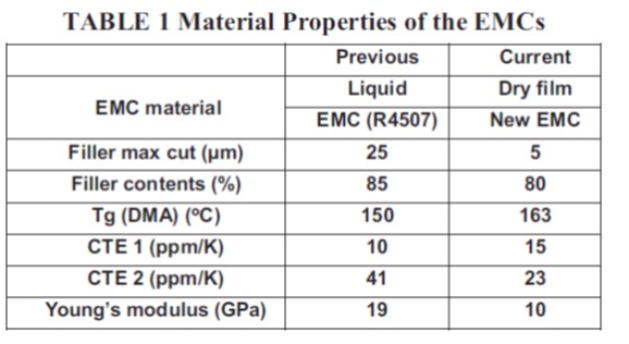
There are a couple key property differences in the two approaches.  First the CTE below Tg (CTE 1 in Table 1) for the Unimicron dry film EMC is 15 ppm/°C which is nearly double the CTE for the Ajinomoto LE series.  The CTE of the EMC is typically closely matched to the CTE of the carrier.  In the Unimicron process, the carrier likely has a CTE in the range for printed circuit boards.  The 15 ppm/°C for the CTE 1 makes sense.  If the panel uses a glass substrate (or other ceramic) with the Ajinomoto LE EMC, then the lower CTE 1 of 7 ppm/°C is appropriate.  Note that the modulus of the two film-based EMC’s are about the same; 7 GPa for the Ajinomoto LE series and 10 GPa for the dry film EMC in the Unimicron process. Another similarity is the Tg’s are very close; 167°C for the Ajinomoto LE series and 163°C for the dry film EMC in the Unimicron process.

References

  1. John Lau et. al. “Feasibility Study of Fan-Out Panel-Level Packaging for Heterogeneous Integrations, 2019 IEEE, 69th Electronic Components and Technology Conference. The authors were part of a consortium consisting of the following companies; Unimicron, ASM Pacific Technology Ltd, Dow Chemical Company, Jiangyin Changdian Advanced Packaging Co., Ltd., Indium Corporation, Huawei Technologies Co. Ltd., Hong Kong University of Science and Technology.
Share on LinkedIn Share

Filed Under: Uncategorized

« Panel Process for Fan Out Wafer Level Packaging: Part Two
This is Our Constitution »

Leave a Reply

Your email address will not be published. Required fields are marked *

Polymer Innovation Blog

I’m Dr. Jeff Gotro and welcome to the Polymer Innovation Blog. Over the last 40 years I have been involved in polymer research, along with product and process development. I acquired invaluable experience working for IBM, AlliedSignal, Honeywell, Ablestik Labs (now Henkel) and in multiple consulting projects. In this blog, I (along with some guest contributors) will share our experiences, tips, and “tricks of the trade” to get more out of your innovation efforts and discuss new trends and technical advances in the polymer industry.
View Jeff Gotro, Ph.D., CMC's profile on LinkedIn

Innocentrix, LLC


Click to Visit Website

plastics expert witness
Click for More Information

Subscribe by Email

Search the Blog

Polymer Video Training

Visit our Video Store

Polymers in Electronic Packaging

polymers in electronic packaging Are you confused about what is electronic packaging? Have you ever wondered what type of polymers and polymer-based composites are used in electronics? Learn More...

Practical Tips for Curing Thermosets

practical tips for curing thermosets Have you ever had a question about the degree of cure or is your part fully cured after processing? Confused about what is gelation or how does vitrification impact thermoset curing? Learn More...

Rheology of Thermosets

rheology of thermosets Have you ever had a question about measuring the rheological properties of thermosets Didn’t know what is the right experimental approach to get the right rheological information? Learn More...

Dielectric Cure Monitoring of Thermosets

Dielectric Cure Monitoring of Thermosets Do you have a need for an in-situ cure monitor for a thermoset process but don’t know where to start? Are you confused about the terminology used in dielectric spectroscopy? Learn More...

Introduction to Biopolymers and Bioplastics

Introduction to Biopolymers and Bioplastics Would you like to know how sustainable are bio-based polymers? Or what is the market size and growth rate for bioplastics? Or have questions about the biomass supply chain? Learn More...

Thermoset Characterization

Thermoset Characterization Have you ever had a question about how to measure a physical property of a thermoset? Confused about what is gelation or how does vitrification impact thermoset curing profiles? Or wondered how to measure the glass transition temperature of an epoxy or polyester composite? Learn More...

Amazon.com Bookshelf

Robert's Rules of Innovation Thermal Analysis of Polymers Order

Copyright © 2025 Innocentrix, LLC · All Rights Reserved