

In the last post we described both non-conductive film (NCF) and wafer applied underfills. In each of these, the underfill is applied to the wafer prior to chip joining to the semiconductor packaging substrate. Thermocompression bonding is used to: Align the chip and the substrate using fiducials using a sophisticated vision system Control the temperature, force and ... [Click to Continue...]
Happy Halloween!

I was at the Irvine Park Railroad Pumpkin Patch (in Orange County California) with my wife, daughter, son-in-law, and my 19 month old grandson last Saturday for some fun at the pumpkin patch. They had a train ride, hay bale maze, kids games, bounce houses, face painting, cookie decorating, tractor races, horse rides, and a bunch of those wooden pictures with holes for your ... [Click to Continue...]
Polymer Challenges in Electronic Packaging: Part 4 Wafer Level Underfills

In the last post we outlined the technical drivers for underfills and showed examples of the first type of non-capillary underfill called No-flow underfill (NUF) and introduced the concept of thermocompression (TC) bonding as the process that yielded the best results in the past. Wafer level underfills are becoming more popular and have two embodiments: Non-conductive ... [Click to Continue...]
Polymer Challenges in Electronic Packaging: Part 3 No Flow Underfills
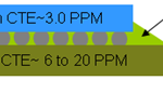
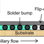
In the last post we discussed capillary underfills which are the mainstay in flip chip packages. However, future technical drivers pose large technical challenges to capillary underfills. The technical drivers for the next generation of underfills are: Bump pitch going to less than 150 microns Bump diameter is moving to less than 50 microns CTE requirements are moving ... [Click to Continue...]
Polymer Challenges in Electronic Packaging: Underfills Part 2
In the previous post we discussed the challenges of capillary underfills. This post will focus on some of the technical aspects required to formulate an effective underfill. As can be seen in the above figure, traditional capillary underfills are typically provided in syringes (or cartridges) and consist of a formulated mixture of thermoset resins and fillers. The resins ... [Click to Continue...]