
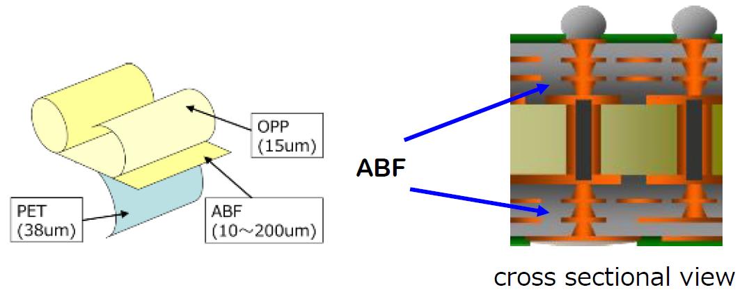
Build-up film technology has been an integral part of high-density interconnect (HDI) circuit boards for decades. As shown in the figure above, the build-up layers are used to fabricate fine lines and stacked vias in high density circuit boards. One supplier is Ajinomoto Fine-Techno and the products they introduced have been termed “ABF” for Ajinomoto Build-Up Films. Sekisui also provides a line of materials for build-up layers (discussed below). All of the build-up films come in a variety of thicknesses and are provided as a film (supported by a PET carrier and release layer, see the image on the left in the figure above). A second type of build-up film is supplied on a copper carrier termed “RCC” for resin coated copper. In recent years, the drive for faster circuits speeds and lower loss has been a driving force in the R&D related to build-up film technology.
The main design features for advanced high-performance build-up films are driven by the following three material properties
- Low CTE to achieve low package warpage
- Low Df for lower transmission loss
- Low surface roughness for lower transmission loss along with finer circuit lines/spaces
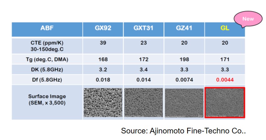
Ajinomoto recently released the GL series which had both a lower coefficient of thermal expansion (CTE) and a lower dielectric loss factor, Df. In order to achieve lower circuit transmission loss, both the Df and the surface roughness of the copper foil need to be reduced. The table below shows the high-performance ABF products. The GL is the newest product in the line-up. Note that the GL has a Df of 0.0044 at 5.8 GHz which is pretty low compared with the GX series (epoxy-based) and close to the GZ41 which is a blend of epoxy and cyanate ester. Cyanate esters typically have lower Df. The exact chemistry of the GL ABF was not disclosed. Note in the table below, the SEM images on the bottom indicate a progessive lowering of the surface profile. Due to the skin effect (the electrical signal propagates along the surface of the copper circuit trace), the smoother the copper surface, the less transmission loss occurs.
Table 1. Ajinomoto Build-Up Film Properties
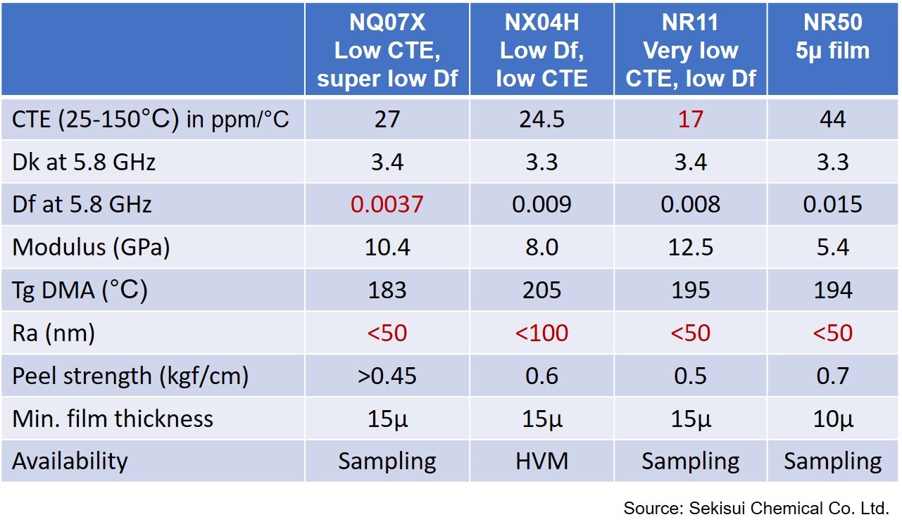
Sekisui Chemical Company also developed a product line of build-up films for use in HDI substrates primarily used in flip-chip BGA’s. Consistent with the three design criteria noted above, the Sekisui build-up films have low CTE, and three of the Sekisui films have low dielectric loss factors. The NR11 product has a CTE of 17 ppm/°C which is matched to copper. The NQ07X has a very low Df, close to the Ajinomoto GL product in Table 1.
Table 2. Sekisui Build-Up Film Properties
The Sekisui build-up films also have low roughness resulting in less transmission loss in operation.
While the typical build-up films from Ajinomoto and Sekisui are supplied as a B-staged film coated on an polyethylene terephthalate (PET) carrier with a top release sheet, Ajinomoto offer a Resin Coated Copper (RCC) product as shown in Figure 1.
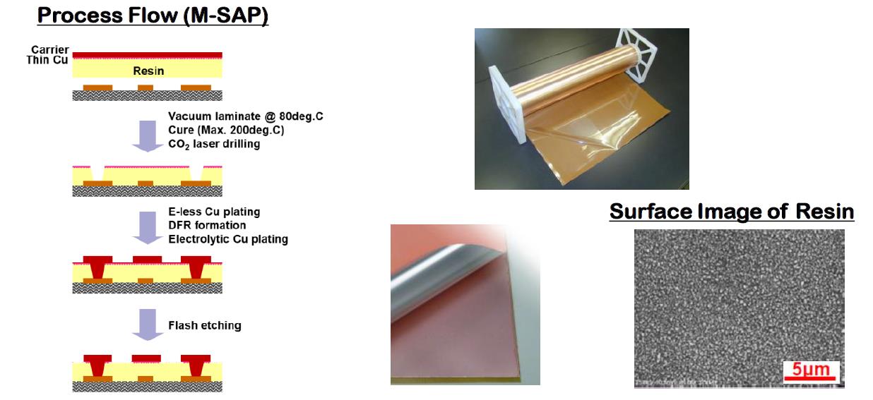
Figure 1. Resin Coated Copper (RCC) process flow for Ajinomoto Fine-Techno
The main feature of the RCC approach is to coat the build-up film on a carrier that has a very thin layer of copper. The details of the coating process and RCC imaging process were discussed in a previous post in this series. The thin layer of copper eliminates the need to sputter a thin copper seed layer prior to laser drilling, thus reducing cost and facilitates fine line formation. The Ajinomoto low Dk/Df RCC shown in Table 3 has a lower Dk and Df compared with the existing RCC products. GX-E4 and GX-E5 had Dk’s in the range of 3.3-3.4 and Df’s in the range of 0.0073 – 0.0093 (use the link to the previous post and look at Table 1 to get a complete listing of the standard RCC products. The physical properties of the low Dk/Df RCC are shown in Table 3.
Table 3. Ajinomoto Low Dk/Df Resin Coated Copper (RCC) Properties

Note that the dielectric constant, Dk is lower than 3.0 and the Df value is also very low, Df=0.004. The CTE is larger than the GX, GZ, and GL products shown in Table 1 potentially indicating the Dk and Df were lowered by using a lower filler loading (the filler loading has a larger impact on the Dk, since silica fillers typically have much higher Dk compared with the epoxy or cyanate ester resins).
In semiconductor packaging, the increasing density, faster signal speeds, and lower transmission losses are driving materials developers to provide build-up films with lower dielectric constants and dielectric loss factors.
Leave a Reply