 In the last post we discussed capillary underfills which are the mainstay in flip chip packages. However, future technical drivers pose large technical challenges to capillary underfills. The technical drivers for the next generation of underfills are:
- Bump pitch going to less than 150 microns
- Bump diameter is moving to less than 50 microns
- CTE requirements are moving towards 20 ppm/C
- Larger die with thousands of bumps or copper pillar interconnects
- Low K ILD (inner layer dielectric) in chip requires stress control and robust bump or pillar joining process
To address the technical challenges, alternate underfill technologies have been developed:
- Dispensable non-conductive pastes for no flow underfill (NCP)
- Non-conductive film (NCF) for no flow underfill
- Wafer level underfills (coat and B-stage on wafer)
- All of the above processes use thermocompression bonding processes
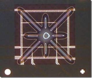
The rest of this post will focus on non-conductive paste (NCP) and the thermocompression (TC) bonding process. NCP is a formulated paste underfill that can be needle dispensed using commonly available die attach adhesive needle dispensing equipment. The first step in the NCP process is to dispense the paste onto the substrate. An example of an NCP dispensed on a substrate can be seen in the following picture (Henkel, presented at the ECTC conference in 2011):
In this case, the typical asterisk pattern is used to ensure good flow and proper fillet formation after the die is placed. The cured Henkel NCP underfill has a CTE of 31 ppm/C and a Tg of 208C by DMA. The chip is attached using thermocompression bonding, with fast bonding time in the order of 4 seconds demonstrated. The NCP has demonstrated MSL Level 3 reliability and showed no voids after 168 hours in HAST (Highly Accelerated Stress Testing), and no voids after 100 cycles in Temperature Cycling Testing (TCT).
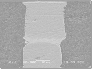
It should be noted that filler entrapment was thought to be a major technical hurdle. Since the NCP is highly filled (typically with silica to lower the CTE while maintaining electrical insulation to prevent interconnect shorting), early reflow processes resulted in silica filler entrapment after the reflow process. With the advent of carefully designed thermocompression (TC) bonding processes, filler entrapment has been eliminated. In the figure to the right, one notices a good bond, good alignment, and no filler entrapment.
The thermocompression bonding process is shown schematically in the following figure (Source: Amkor)

The NCP is dispensed onto the heated substrate. The TC bonder vision system then aligns the die with the substrate using fiducials on the front of the die and on the substrate. The TC bonder then places the interconnect (either bumps or more commonly copper pillars) in contact the the pad on the substrate. Using a controlled force, the temperature is ramped very quickly causing several actions to occur:
- The flux (part of the NCP formulation) is activated to enable fluxing of the interconnects
- A metallurgical bond is made in the interconnects
- The NCP flows, wets the die and the interconnects and begins to rapidly cure
Critical elements of the TC process are proper fluxing (without voiding), good interconnection (formation of metallurgical bonds), and no voiding during the curing of the NCP. The manufacturing process throughput requirements are driving a 3-4 second total bonding time. This is a huge challenge given the three technical requirements above. Several equipment suppliers such as Toray and Panasonic have developed very sophisticated TC bonders for high volume manufacturing. At the present time, the Henkel NCP is commercially available and some OSATs have begun using TC bonding in volume manufacturing.
In the next several posts we will address the many embodiments of wafer level underfills.


Leave a Reply