
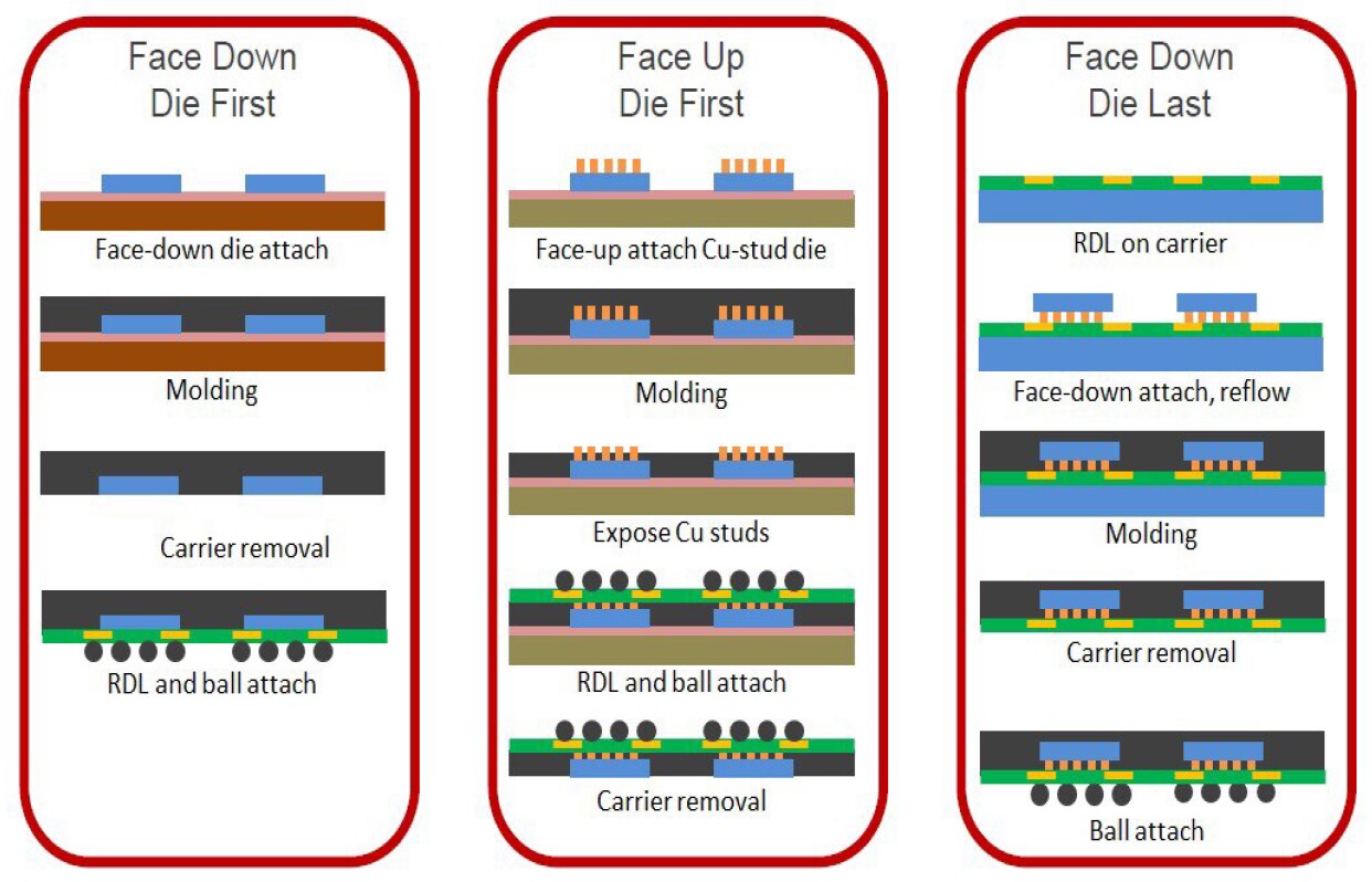
Figure 1. Three process flows for fan-out wafer level packaging (source: SPIL)
The previous post introduced the three types of process flows for fan-out wafer level packaging as seen in Figure 1. This post will describe in more detail the face-down die first process and the face-up, die first approach. For the reader new to fan-out wafer level processing, the face-down die first was introduced by Infineon and was the first FOWLP package in volume production. A more detailed process flow for the die-first face up is shown in Figure 2.
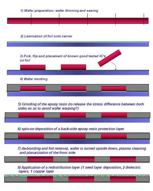
Figure 2. Die-first face down FOWLP process flow (Source: Infineon)
One of the polymer related issues that arose during the development of the process shown in Figure 2 was a coplanarity issue of the chip, mold compound and the RDL after processing. The foundation of the Infineon eWLB process was embedding the known good die face down into a temporary adhesive to form the reconstituted wafer (step 3 in Figure 2). In order for the dies not to move during the epoxy molding process (step 4 in Figure 2), enough force was required to make a good adhesive bond between the die face and the temporary adhesive. The bonding force during the chip placement caused the chip to sink into the adhesive layer. After molding and removal of the carrier foil (along with the temporary adhesive) as shown in step 7 in Figure 2, the polymer dielectric used for the redistribution layers are applied and imaged as shown in step 8 in Figure 2.
During the molding process, the face of the chip is slightly embedded in the temporary adhesive, a small step is formed after the redistribution layers are patterned. Figure 3 shows a SEM image of the coplanarity issue.
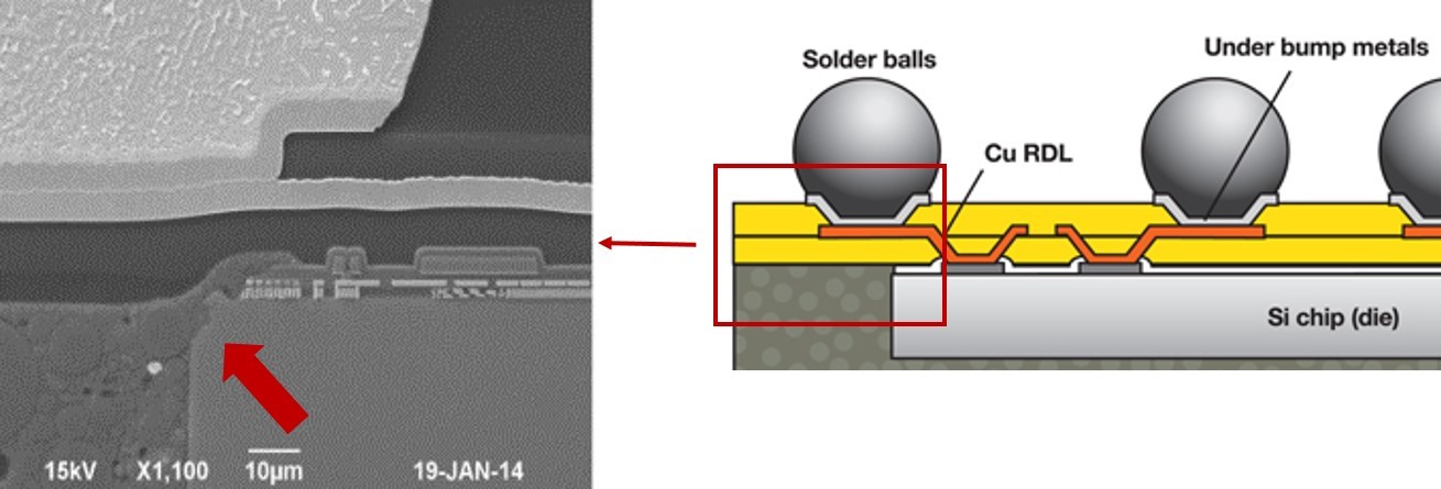
Figure 3. SEM image showing the coplanarity issue after RDL and bumping.
In the ideal world, the chip top surface and the mold compound would be planar as shown in the cartoon on the right in Figure 3. The SEM image on the left in Figure 3 shows an actual cross-section of the area near the edge of the chip. The step in the RDL layer is indicated by the red arrow. One of the features of the RDL material is the ability to flow and adhere well to the epoxy mold compound along with planarizing the step at the corner of the chip. In Figure 3, the RDL effectively planarized the small step and RDL is fairly planar. RDL planarity is important during the solder ball reflow process. The SEM image in Figure 3 shows the solder ball connection is good. The image in Figure 3 is an example of a two layer RDL structure.
A solution to this issue was to use a face-up die first approach. Known good die are plated with a copper stud prior to placing on the temporary adhesive/carrier wafer (see the middle process flow in Figure 1). The epoxy molding process subsequently encapsulates the face-up chip. In order to make an interconnect, the top surface of the molded reconstituted wafer is ground down to expose the tops of the plated copper pillars. The next step is to apply the redistribution layers using the same type of process flow used in the face-down die first approach.
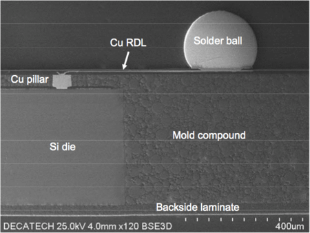
Figure 4. SEM image of a cross-section from a face-up die first process flow (Source: Deca Technologies in Reference 1)
The key feature in Figure 4 is the planar surface onto which the RDL layers were patterned. The grinding operation after molding ensures that the exposed copper pillar is planar with the epoxy mold compound surface thus eliminating the step discussed in Figure 3. The main reason for using the face-up die first approach is to allow the use of what Deca calls Adaptive Patterning. The details of the Deca approach is given in Reference 1. Click on link to access the Deca paper.
References
- Implementation of a Fully Molded Fan-Out Packaging Technology, B. Rogers, S. Scanlan, and T. Olson, originally published by the SMTA for IWLPC 2013, and was presented at the DoubleTree Hotel in San Jose on November 7, 2013
Leave a Reply