Polymer Innovation Blog

Practical tips and advice for polymer, innovation and product development professionals

Polymer Innovation
  • Home
  • eBooks
    • Polymers in Electronic Packaging
    • Rheology of Thermosets eBook
    • Practical Tips for Curing Thermosets
    • Thermoset Characterization
    • Dielectric Cure Monitoring of Thermosets
    • Introduction to Biopolymers and Bioplastics
  • Videos
    • Core Curriculum: 3 Part Video Series
    • Characterization of Thermosets: 4 Part Video Series
    • Advanced Thermoset Cure Kinetics: 3 Part Video Series
    • DSC of Polymers: 5 Part Video Series
    • Thermoplastics: 5 Part Video Series
  • Services
    • Consulting
    • Polymer Expert Witness
  • Learning Center
    • White Paper
  • Why Jeff?
    • Speaker Info
  • Contact
  • Subscribe
  • Members
    • Login
    • Logout

Polymers in Electronic Packaging: Introduction

January 8, 2018 By Jeffrey Gotro Leave a Comment

Happy New Year and Best Wishes for a Prosperous 2018!

Last year I had a series of posts on specific uses of polymers in electronic packaging.  I am in the process of developing an eBook on this topic and have identified new content that I want to include.  I will add the content during my weekly blog posts and then complete the eBook later in the year .

Let’s get started by defining the term electronic packaging.  When I first got into this field, the nomenclature was confusing.  Electronic packaging comprises the materials and structures used to connect the semiconductor chip with other electronic components.  It does not mean the plastic case or in some of the new phones the composites shells.  The semiconductor chips have output and output terminals (called I/O’s) that are used to connect the chip with other chips or with power, resistors, inductors, and capacitors.  The spacing between the I/O’s on the chip (called the pitch) is very small compared with the typical pitch on a printed circuit board.  In order to “fan-out” from the small pitch on the chip to the larger pitch on the substrate or circuit board, electronic packaging designs are used.  Polymers are the enabling technology, whether it be polymer-based adhesives used to glue the semiconductor chips to a metal leadframe and the mold compound used to encapsulate the chip after being mounded as shown in the following schematic.

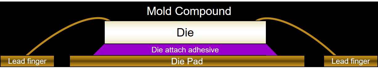
The semiconductor chip, also called a die (strange name, but as you will see, there are a lot of unique terms used in electronic packaging) is attached to the metal die pad with an filled-polymer adhesive called a die attach.  (Click on the hyperlinks to go previous blog posts). The die pad and lead fingers are part of what is called a leadframe.  The leadframe and die are encapsulated using a mold compound (black encapsulant in the image above).  Mold compounds are highly filled epoxy resins.

Other types of packages, such as a flip chip package shown in the next schematic have many polymers used in the design.

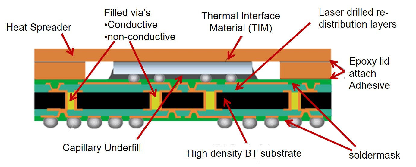
The image above shows a fairly complex flip chip package with many polymers providing critical functions as outlined below:

  • Epoxy, polyimide or polybenoxazole film redistribution layers
  • Bis-maleimide triazine epoxy (BT) laminate used in flip chip high density BT substrates
  • Epoxy/acrylate UV imageable soldermask
  • Silicones/thermal greases in TIM materials
  • Epoxy or cyanate ester/epoxy used in capillary underfills
  • Filled-epoxy via fills (conductive with silver filler and non-conductive with silica filler)

Note the wide range of polymers used.  One of the key aspects of polymers utilized in electronic packaging is high temperature stability along with the ease of processing.  The next post will discuss the advantages of polymers called thermosets in electronic packaging.


Share on LinkedIn Share

Filed Under: Uncategorized

« Happy Holidays
Polymers in Electronic Packaging: What Types of Polymers are Used? »

Leave a Reply

Your email address will not be published. Required fields are marked *

Polymer Innovation Blog

I’m Dr. Jeff Gotro and welcome to the Polymer Innovation Blog. Over the last 40 years I have been involved in polymer research, along with product and process development. I acquired invaluable experience working for IBM, AlliedSignal, Honeywell, Ablestik Labs (now Henkel) and in multiple consulting projects. In this blog, I (along with some guest contributors) will share our experiences, tips, and “tricks of the trade” to get more out of your innovation efforts and discuss new trends and technical advances in the polymer industry.
View Jeff Gotro, Ph.D., CMC's profile on LinkedIn

Innocentrix, LLC


Click to Visit Website

plastics expert witness
Click for More Information

Subscribe by Email

Search the Blog

Polymer Video Training

Visit our Video Store

Polymers in Electronic Packaging

polymers in electronic packaging Are you confused about what is electronic packaging? Have you ever wondered what type of polymers and polymer-based composites are used in electronics? Learn More...

Practical Tips for Curing Thermosets

practical tips for curing thermosets Have you ever had a question about the degree of cure or is your part fully cured after processing? Confused about what is gelation or how does vitrification impact thermoset curing? Learn More...

Rheology of Thermosets

rheology of thermosets Have you ever had a question about measuring the rheological properties of thermosets Didn’t know what is the right experimental approach to get the right rheological information? Learn More...

Dielectric Cure Monitoring of Thermosets

Dielectric Cure Monitoring of Thermosets Do you have a need for an in-situ cure monitor for a thermoset process but don’t know where to start? Are you confused about the terminology used in dielectric spectroscopy? Learn More...

Introduction to Biopolymers and Bioplastics

Introduction to Biopolymers and Bioplastics Would you like to know how sustainable are bio-based polymers? Or what is the market size and growth rate for bioplastics? Or have questions about the biomass supply chain? Learn More...

Thermoset Characterization

Thermoset Characterization Have you ever had a question about how to measure a physical property of a thermoset? Confused about what is gelation or how does vitrification impact thermoset curing profiles? Or wondered how to measure the glass transition temperature of an epoxy or polyester composite? Learn More...

Amazon.com Bookshelf

Robert's Rules of Innovation Thermal Analysis of Polymers Order

Copyright © 2025 Innocentrix, LLC · All Rights Reserved