 In the last post we described both non-conductive film (NCF) and wafer applied underfills. In each of these, the underfill is applied to the wafer prior to chip joining to the semiconductor packaging substrate. Thermocompression bonding is used to:
- Align the chip and the substrate using fiducials using a sophisticated vision system
- Control the temperature, force and Z-axis travel during the bonding process
- Rapidly simultaneously reflow the interconnection (solder bump and increasingly more popular is the copper pillar)
- Provide the proper temperature profile to allow fluxing (flux included in the underfill formulation), softening and wetting of the underfill around the interconnection
- Curing of the polymer-based underfill (either film or wafer applied)
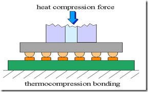
The process schematic is given in the following figure:
The thermocompression process challenges are:
- Significant process development and optimization required
- Lead-free solder reflow process is tough on organic polymer-based underfills
- Requires very fast bonding times for optimal manufacturing throughput
- Vision systems are required for precise chip-to-substrate alignment
- Capital intensive for volume production
- Yield optimization is a key cost driver since this process is used for chips with very high bump or copper pillar counts
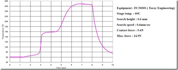
The figure below shows a typical temperature profile for a thermocompression bonding process:
Source: Namics, International Microelectronics and Packaging Society (IMAPS) 2013, Orlando Florida
The substrate on the stage is preheated to approximately 60C. The bonding process starts and the temperature is rapidly ramped to 160C to allow the nonconductive paste, wafer level underfill, or NCF to soften and begin to flow. The temperature is subsequently increased to approximately 270C and held for several seconds allowing the copper pillar with a lead-free solder cap to reflow. The lead-free reflow temperature will cause significant voiding in the underfill if the curing reactions and formulation chemistry is not optimized for the high temperature ramping. The bonder then quickly cools the joined package to approximately 80C. The entire bonding process occurs in about 10 seconds.
The key process steps are:
- Ensuring proper alignment prior to the TC bonding step
- Controlling the Z-axis height to maintain the proper interconnect height
- Controlling the contact force and limiting the maximum force (when the solder reflows, if the bonding force is not controlled, too much flow may occur)
- Providing for precise temperature control during the two-step temperature profile
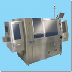
Toray Engineering and Panasonic have developed very sophisticated TC bonders. An example from Toray Engineering is the FC3000 (used in the process profile above):
In the next post we will dive into embedded wafer level packaging (eWLB, or eWLP, or a number of other trade names used by various OSATS).
I will be attending the International Wafer Level Packaging Conference (IWLPC) in San Jose November 5-7, 2013 and will report on recent advances from the conference in future posts.


This is a good technical introduction to a timely topic.
Mass production thermo-compression bonding is the “next frontier” and this equipment application is finally getting serious orders behind it.
Chip Scale Review states there are 21 equipment players of varying capabilities in the market. While in December, K&S announced to their customer-base that they are an “interconnect company” and are entering the TCB game too.
Sophisticated wafer handling techniques, for thinning and maintaining flatness and throughput will be important. The competition for the best equipment and assembly process flow, seems to be wide open.