
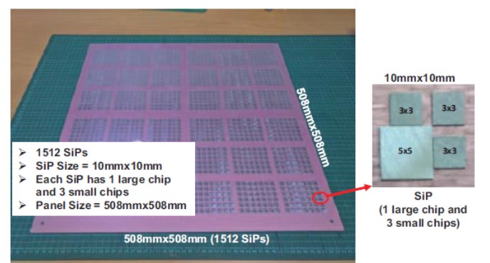
Figure 1. Unimicron UniSIP panel for heterogeneous integration (from ref [1]).
The Unimicron process (UniSIP) for heterogeneous integration in panel-level fan out packaging uses printed circuit board processes with a panel size of 508 mm x 508 mm as shown in Figure 1 (from ref [1]). An interesting side-note here is that this is what I consider a system-in-package (SiP). At the SiP conference June 25-27 in Monterrey, CA, there were many papers describing both system-in-package and system-in-modules. The system-in-module approach has been around for decades, where multiple different chips are mounted on a module. For the older crowd here, remember the multichip modules (MCM) back in the 1990’s?
As shown in Figure 1, the UniSIP process packages four different dies in a single package. The demonstration panel uses four dies in a 10mm x 10 mm SiP package. Each panel has 1512 SiPs. The Unimicron UniSiP process uses a HDI-type printed circuit board process. More details are presented in reference [1].
Consistent with a PCB approach, UniSIP approach uses Ajinomoto build-up films for dielectric layers one and two (ABF DL1 and ABF DL2) as shown in Figure 2.
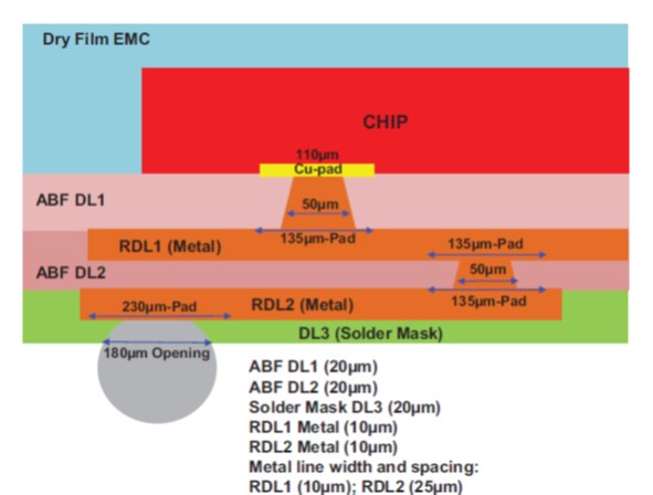
Figure 2. Cross-section of the Unimicron UniSiP panel (ref [1])
None of the current FOWLP on round wafers use an Ajinomoto build-up material for the RDL dielectric. In the High-Density Interconnect (HDI) circuit board process, build-up films from Ajinomoto, Sekisui, and others are extensively used. Previous posts discussed the build-up films used in HDI.
For the UniSiP process, the authors claim that to reduce warpage, the CTE of the ABF should be closely matched to the CTE of the ECM panel (which consists of a core substrate with embedded dies on each side) [1]. The properties of the ABF used in the panel process are given in Table 1.
Table 1.

From a materials perspective, there are a couple things to note. The filler content remains high at 80 wt %, but the maximum filler size has been significantly reduced. The smaller filler size was necessary to aid in achieving finer line and spaces in the RDL. With the traditional ABF (noted at Old ABF in Table 1), the RDL thickness was 25 µ resulting in a lines/space resolution of 20 µ. With the finer filler (5µ and a thinner RDL of 12 µ) the resolution was improved to 5µ (on a glass substrate). The process to use the Ajinomoto build up films for the RDL layers is shown in Figure 3.
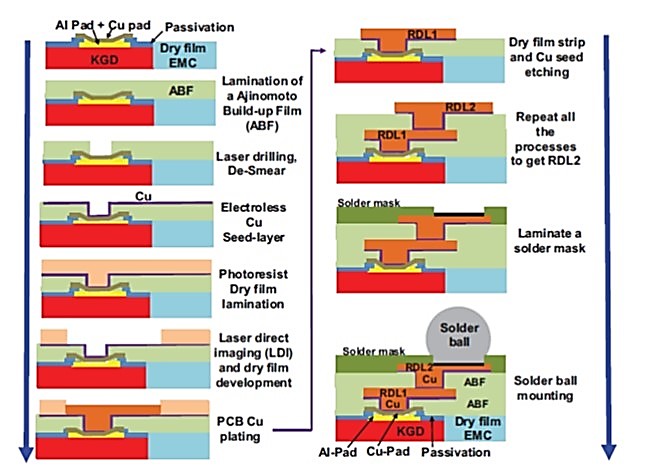
Figure 3. UniSiP RDL process using the improved Ajinomoto Build-Up Film (from ref [1])
The RDL process is very similar to that used in HDI printed circuit board fabrication.
One potential drawback of using the ABF approach is the surface roughness of the RDL layer. In Figure 4, an SEM image of the lines on the Ajinomoto ABF is shown.
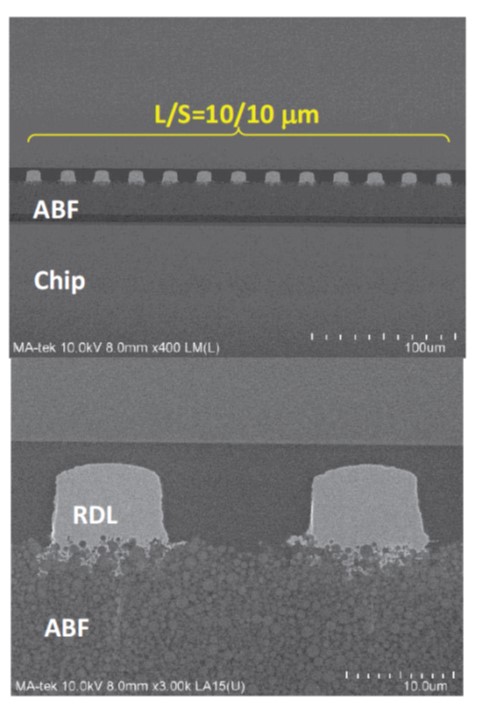
Figure 4. SEM images of a cross-section of the RDL layer in the UniSiP process (from ref [1])
On the positive side, the lower surface roughness allows for 10 µ lines and spaces as seen in the top part in Figure 4. On the other hand, lower surface roughness typically leads to lower copper peel strength (adhesion of the copper trace to the ABF). The lower portion in Figure 4 shows a higher magnification of two copper traces in the RDL. The presence of a high filler loading is clearly visible. Additionally, there is plated copper that appears to penetrate into the RDL layers. The copper penetration could increase the peel strength due to mechanical interlocking. A potential downside is that if the filler/resin adhesion is not optimized, there potentially could be filler pull-out during the peel testing. There also appears to be some copper migration (or incomplete seed layer etching) visible between the two traces in Figure 4.
The work by the consortium described in the ECTC paper by John Lau and his colleagues shows nice progress in understanding the key issues and challenges in panel-level processing for heterogeneous packages.
References
- John Lau et. al. “Feasibility Study of Fan-Out Panel-Level Packaging for Heterogeneous Integrations, 2019 IEEE, 69th Electronic Components and Technology Conference. The authors were part of a consortium consisting of the following companies; Unimicron, ASM Pacific Technology Ltd, Dow Chemical Company, Jiangyin Changdian Advanced Packaging Co., Ltd., Indium Corporation, Huawei Technologies Co. Ltd., Hong Kong University of Science and Technology.

The expanded and updated eBook on “Rheology of Thermosets is available. The eBook covers both the rheology of uncured thermosets which is important in dispensing applications as well as the chemorheology during curing. Click here to get your copy.
Leave a Reply