Guest Post by Huan Lee, Lambient Technologies
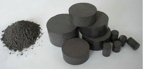
Normally available in either B-staged powders or pellets for transfer molding, epoxy molding compound (EMC) is essential for electronics packaging and is used to encapsulate billions of integrated circuits each year.
Figure 1. Granular (left) and pelletized (right) epoxy molding compound [Ref. 1]
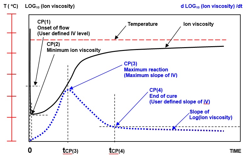
During cure of EMC, when monomers react to form polymer chains and then a network, the electrical resistivity, also known as ion viscosity, behaves like a typical thermoset as shown in Figure 2.
Under isothermal conditions the material heats quickly to the processing temperature, and mechanical viscosity suddenly decreases as it softens or melts. Mobile ions experience less resistance to movement and in response ion viscosity suddenly decreases. At this point curing begins and the cure rate increases as the reaction accelerates. Ion viscosity increases continuously as the concentration of unreacted monomers diminishes. Toward the end of cure, the reaction rate decreases, reflected in the decreasing slope of ion viscosity, and eventually the slope reaches a value of zero when cure has stopped completely.
Critical Points, identified in Figure 2, can characterize the curves for ion viscosity and slope of ion viscosity, and we will see in the next post how Critical Points provide valuable insight into the dynamics of cure.
Figure 2. Ion viscosity and slope of ion viscosity during isothermal processing
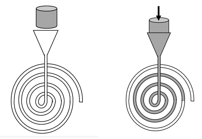
The viscosity and curing behavior of EMC vary with the hundreds of available formulations. The high-speed, high-volume requirements of manufacturing demand consistent, reliable material performance and EMC is commonly evaluated with the spiral flow test, schematically illustrated in Figure 3. In this test, EMC with a specified charge mass, mold temperature and transfer plunger speed is injected into a mold with an Archimedean spiral channel. As material flows through the channel, it cures, undergoes gelation and finally solidifies enough to stop flow. The length of the cured portion is a measure of the combined characteristics of fusion under pressure, melt viscosity and gelation rate under the test conditions.
Figure 3. Spiral flow test with mold before test (left) and after test (right)
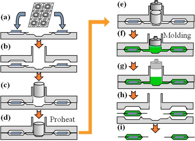
Integrated circuits are manufactured with steps similar to those of Figure 4, in which EMC is heated until it melts then is injected into a mold with cavities for each integrated circuit. With a process temperature usually between 160 °C and 180 °C, the EMC must flow with low viscosity to avoid damaging delicate wire bonds and must fill the mold before gelation. The speed of cure is critical—too fast, and the EMC gels before filling the mold; too slow, and processing time is wasted.
To maximize productivity, parts are removed from the mold when the EMC has reached about 40% epoxy conversion and is rigid enough to retain its form. Then they are baked in ovens at about 175 °C for an additional three or four hours until full cure.
Although the spiral flow test roughly emulates this process up to the gel point, it gives little insight into how the material cures. Nevertheless, if a manufacturer has established that consistent, specific results of the spiral flow test correspond to well molded products, then any change in test results is a warning that the EMC is not behaving as required.
Figure 4. Steps in the EMC transfer molding process for electronic packaging [Ref. 2]
Dielectric cure monitoring (DEA) can provide valuable additional information for quality control and manufacturing. The viscosity of EMC and the result of the spiral flow test depend on how the resin cures as well as how it interacts mechanically with the filler, which often consists of spherical silica particles. The cure of EMC, however, depends only on the resin, which is commonly epoxy cresol novolac with phenolic curing agents. By observing only resin cure, DEA can isolate one of the critical variables which determines how EMC fills the mold. In addition, DEA can be performed with sensors in the mold itself, to measure EMC cure during manufacturing—unlike the spiral flow test, which must be in a lab with a setup and conditions much different from an IC package mold.
References
- Epoxy molding compound picture credit: Shyama Construction & Waterproofing Co., Kolkata, West Bengal, India
- Molding process picture credit: Huang, Wan-Chiech; Hsu, Chao-Ming and Yang, Cheng-Fu, “Recycling and Refurbishing of Epoxy Packaging Mold Ports and Plungers,” Inventions 2016, 1(2), 11; https://doi.org/10.3390/inventions1020011, June 6, 2016

Hello,
We are a small IC packaging facility,
we are using Besi BV for molding and we are looking for a solution to characterize the properties of the molding materials. Do you have a solution for such tests including spiral flow ? if yes, could you please share some data and pricing ?
thank you