
To all my loyal readers, thank you for you interest in my blog. To all, have a safe and relaxing holiday season. Take some time to be with family and friends and enjoy some time off. I will be on vacation until Jan 2, 2019, so my next post will be on Monday January 7, 2019 (whew, where did 2018 go?). After the holidays, we will dive back into mixing and dispersion methods ... [Click to Continue...]
Polymers in Electronic Packaging: New Advances in Build-up Technology
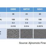
Build-up film technology has been an integral part of high-density interconnect (HDI) circuit boards for decades. As shown in the figure above, the build-up layers are used to fabricate fine lines and stacked vias in high density circuit boards. One supplier is Ajinomoto Fine-Techno and the products they introduced have been termed “ABF” for Ajinomoto Build-Up Films. Sekisui ... [Click to Continue...]
Polymers in Electronic Packaging: Fan-Out Wafer Level Packaging Part Five
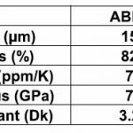
The last post described some of the new developments in film-based epoxy mold compounds from Hitachi Chemical (EBIS) and Ajinomoto (see image above courtesy of Ajinomoto Fine-Techno). The main driver for panel level processing is to reduce cost. Another area where there is an opportunity to reduce cost is in the redistribution layer process. The main dielectrics used in ... [Click to Continue...]
Happy Thanksgiving
Wishing all my readers a safe and Happy Thanksgiving. Use the holiday break to enjoy time with family and friends. Watch some football and don't eat too much turkey! OK, have at it if you must! ... [Click to Continue...]
Polymers in Electronic Packaging: Fan-Out Wafer Level Packaging Part Four
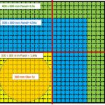
The last post discussed the future transition to a panel format for Fan-Out Wafer Level Packaging. The transition will occur over the next several years as the volumes ramp for wafer level packages. Yole' Developpement has investigated the potential timing for the panel process. Figure 1 shows the timing of panel R&D, sampling and low-volume manufacturing (LVM) and ... [Click to Continue...]