
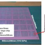
Figure 1. Unimicron UniSIP panel for heterogeneous integration (from ref [1]). The Unimicron process (UniSIP) for heterogeneous integration in panel-level fan out packaging uses printed circuit board processes with a panel size of 508 mm x 508 mm as shown in Figure 1 (from ref [1]). An interesting side-note here is that this is what I consider a system-in-package (SiP). At ... [Click to Continue...]
Happy Fourth of July
Happy Fourth of July Have a safe and relaxing Fourth of July ... [Click to Continue...]
This is Our Constitution

I picked up a great little book and read it on one of my cross-country flights a couple weeks ago. It's called "This is Our Constitution" written by Khizr Khan. Khizr Khan is a Muslim immigrant, United States citizen, Harvard Law School graduate, and a Gold Star Father. His son US Army Captain Humayun Khan was killed in action in 2004 while stopping a suicide attack ... [Click to Continue...]
Panel Process for Fan Out Wafer Level Packaging: Part Three, Film Epoxy Mold Compounds
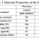
Figure 1. Cross-section from the Unimicron process from reference [1]. The last post discussed the dry film EMC using a printed circuit board vacuum lamination approach. The panel size was 508 mm x 508 mm [1]. Panel level processing will ultimately result in lower cost per unit. What will be some of the major technical challenges? The epoxy molding compound (EMC) ... [Click to Continue...]
Panel Process for Fan Out Wafer Level Packaging: Part Two
This post will focus on some of the emerging technologies being developed for fan-out panel level (FO-PLP) processing. The epoxy molding process for fan-out wafer level packaging (FO-WLP on the lower part in the image above) used compression molding of either liquid or powdered epoxy mold compound (EMC). The process and materials were optimized to provide uniform thickness ... [Click to Continue...]