To all my loyal readers, have a safe and relaxing Labor Day Weekend. ... [Click to Continue...]
Polymers In Electronic Packaging: Non-Conductive Film Underfill, Part Two
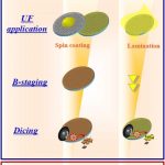
Figure 1. Non-conductive film (NCF) process flow (courtesy of Dow, ref [1]) The last post provided an introduction to non-conductive film used in wafer-level underfill. The image above from Dow Electronic Materials shows the overall process flow for a NCF. For the most part, the NCF materials are used in conjunction with copper pillar interconnects as shown in the top ... [Click to Continue...]
Polymers In Electronic Packaging: Non-Conductive Film (NCF) Underfill
Figure 1. Non-conductive Film process flow The last post described the technical challenges when using capillary underfills. Pre-applied underfills or wafer-applied underfills are being developed. There are three types of pre-applied underfills: Wafer level underfills that are coated onto the wafer and B-staged Non-conductive paste (NCP) that is dispensed onto the ... [Click to Continue...]
Polymers In Electronic Packaging: Introduction to Wafer-Level Underfill
Image from DuPont Electronic Solutions [1]. A previous post described the challenges associated with the future use of capillary underfills. The technical drivers for the next generation of underfills are: Bump pitch going to less than 100 microns Bump diameter is moving to less than 50 microns CTE of the underfill needs to be in the range of 20 ppm/°C Large ... [Click to Continue...]
Panel Process for Fan Out Wafer Level Packaging: Part Four, Build-Up Films for Redistribution Layers (RDL)
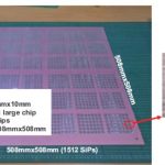
Figure 1. Unimicron UniSIP panel for heterogeneous integration (from ref [1]). The Unimicron process (UniSIP) for heterogeneous integration in panel-level fan out packaging uses printed circuit board processes with a panel size of 508 mm x 508 mm as shown in Figure 1 (from ref [1]). An interesting side-note here is that this is what I consider a system-in-package (SiP). At ... [Click to Continue...]
