
This post will focus on some of the emerging technologies being developed for fan-out panel level (FO-PLP) processing. The epoxy molding process for fan-out wafer level packaging (FO-WLP on the lower part in the image above) used compression molding of either liquid or powdered epoxy mold compound (EMC). The process and materials were optimized to provide uniform thickness across the wafer with no flow marks. Two considerations needed to be addressed when evaluating EMC’s for panel process:
- The panel size is typically in the 500-600 mm on a side, which is much larger than the 300 mm round wafer. The larger panel size is one of the main drivers for lowering the cost.
- The flow of liquid EMC’s in a square or rectangular panel will lead to non-uniform flow paths (center to corner is longer than center to edge) and thickness variations from center to corners.
In Figure 1 (courtesy of Amkor/Nanium) the liquid EMC is dispensed in the middle of the wafer prior to compression molding.
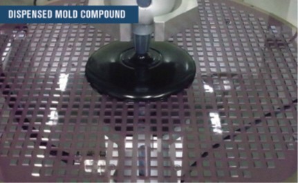
Figure 1. Dispensing of a liquid epoxy mold compound onto the re-constituted round wafer (courtesy of Amkor/Nanium)
The flow path is uniform radially and the compression molding process was optimized to minimize flow marks and obtain a uniform thickness from center to edge. The properties of the liquid or granular EMC for the wafer level compression process was tailored to achieve uniform thickness and have low warpage after curing.
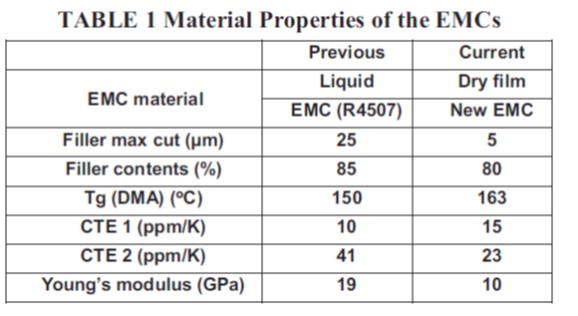
Some panel processes used liquid EMC’s (Nagase R4507) in a modified compression molding process during the initial prototyping stages [1]. Subsequent work has investigated the use of a dry film epoxy mold compound [2].
The advantages of using dry film epoxy molding compounds are [2]:
- Better control of the top surface flatness after molding
- More uniform thickness from center to corners
- Uses a printed circuit board process (vacuum lamination)
- Has higher throughput
- Less particle contamination
Figure 2 shows a schematic of the final fan-out panel level package made using the Unimicron process with dry film EMC. The panel size was 508mm x 508 mm which necessitated a lamination type process for the EMC.
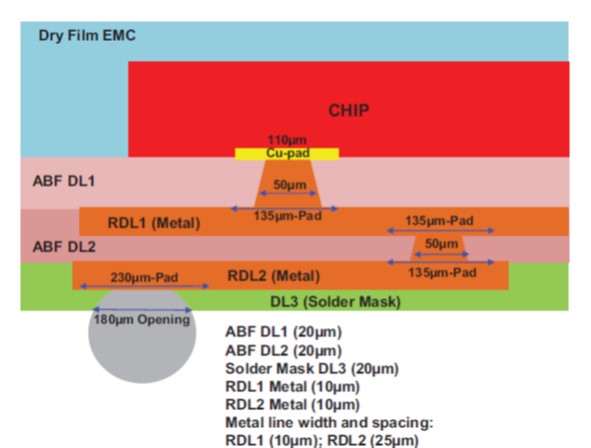
Figure 2. Cross-section from the Unimicron process from reference [2].
In Figure 2, there are several materials to note. The approach has been to use a printed circuit board process as much as possible, both to lower cost and leverage the PCB processes and expertise of the member companies. The details of the Uni-SIP process are given in reference [2]. The properties of the dry film EMC are compared with the Nagase liquid EMC in Table 1 (from ref [2]).
The chips are mounted face-down on a temporary carrier with a two-sided thermal release layer forming the re-constituted panel. The dry film EMC is vacuum laminated on top of the carrier and chips using a two-stage vacuum lamination process using Nikko-Materials equipment. The first stage is vacuum lamination at 100°C for 30 seconds at a pressure of 0.68 MPa which allows the dry film to flow and encapsulate the chips. The second step followed by what is called a “flattening press” at 100°C for 60 seconds at a pressure of 0.54 MPa to ensure the surface of the dry film is flat.
The details of the Nikko-Materials lamination press may be found at https://www.nikko-materials.com/en/cvp300_en#main
After the lamination process, the EMC is partially cured (most likely beyond the gel point to allow a stand alone post cure process). The laminated panel is then post cured at 150°C for 1 hour followed by 30 minutes at 180°C [2]. In Table 1, note that the Tg for the dry film EMC is 163°C. As we have discussed in several previous posts, the cure temperature should typically be above the fully cured Tg. In this process, we observe that the final post cure is done above the fully cured Tg and should lead to a consistent Tg after post cure. The filler size is reduced in the dry film EMC and the filler loading is also slightly lower, most likely to improve the flow during vacuum lamination. The lower filler loading leads to an increased CTE and lower Young’s modulus as would be expected from the lower filler loadings. The Tg is governed by the resin matrix, and the details of the resin chemistry were not disclosed.
The second material to note is the use of Ajinomoto build-up films for dielectric layers one and two (ABF DL1 and ABF DL2). None of the current FOWLP on round wafers use an Ajinomoto build-up material for the RDL dielectric. In the High-Density Interconnect (HDI) circuit board process, build-up films from Ajinomoto, Sekisui, and others are extensively used. The use of build-up films will be covered in a subsequent post.
References
- John Lau, et. al., Chip-First Fanout-Out Panel-Level Packaging for Heterogeneous Integration, IEEE Transaction on Components, Packaging and Manufacturing Technology, Vol. 8, No. 9, September 2018, p. 1561
- John Lau et. al. “Feasibility Study of Fan-Out Panel-Level Packaging for Heterogeneous Integrations, 2019 IEEE, 69th Electronic Components and Technology Conference. The authors were part of a consortium consisting of the following companies; Unimicron, ASM Pacific Technology Ltd, Dow Chemical Company, Jiangyin Changdian Advanced Packaging Co., Ltd., Indium Corporation, Huawei Technologies Co. Ltd., Hong Kong University of Science and Technology.

The expanded and updated eBook on “Dielectric Cure Monitoring of Thermosets is available. The eBook describes some very interesting practical applications for dielectric cure monitoring in SMC, BMC and autoclave processes. Click here to get your copy.
Leave a Reply