Polymer Innovation Blog

Practical tips and advice for polymer, innovation and product development professionals

Polymer Innovation
  • Home
  • eBooks
    • Polymers in Electronic Packaging
    • Rheology of Thermosets eBook
    • Practical Tips for Curing Thermosets
    • Thermoset Characterization
    • Dielectric Cure Monitoring of Thermosets
    • Introduction to Biopolymers and Bioplastics
  • Videos
    • Core Curriculum: 3 Part Video Series
    • Characterization of Thermosets: 4 Part Video Series
    • Advanced Thermoset Cure Kinetics: 3 Part Video Series
    • DSC of Polymers: 5 Part Video Series
    • Thermoplastics: 5 Part Video Series
  • Services
    • Consulting
    • Polymer Expert Witness
  • Learning Center
    • White Paper
  • Why Jeff?
    • Speaker Info
  • Contact
  • Subscribe
  • Members
    • Login
    • Logout

Polymers in Electronic Packaging: Fan-Out Wafer Level Packaging Part Five

December 3, 2018 By Jeffrey Gotro 1 Comment

The last post described some of the new developments in film-based epoxy mold compounds from Hitachi Chemical (EBIS) and Ajinomoto (see image above courtesy of Ajinomoto Fine-Techno).  The main driver for panel level processing is to reduce cost.  Another area where there is an opportunity to reduce cost is in the redistribution layer process.  The main dielectrics used in wafer-based fanout is photosensitive polyimides and polybenzoxazole (PBO) positive tone resists.  A commonly used positive tone photosensitive PBO is HD8940 (Hitachi DuPont).  A challenge has been to lower the cure temperature of the PBO and polyimides to be less harsh on the epoxy mold compounds.

High temperature processing of the photosensitive dielectrics will be an even bigger challenge in panel level processing.  The panel process will initially use a printed circuit board type process flow which entails lower temperature processes.  With this in mind, Dr. John Lau at ASM Pacific has been leading a consortium investigating panel level processing.   The consortium includes ASM, Dow, Huawei, Indium, JCET and Unimicron.  The team recently published an interesting paper describing the printed circuit board approach to panel level fanout [1].  The paper demonstrates several concepts that will be important for panel level processing:

  • Dry film epoxy mold compound
  • Build up films used as dielectrics for redistribution layers (RDL1 and RDL2)
  • Heterogeneous integration of 4 chips into the fanout package
  • Demonstration of a new assembly process called uni-substrate-integrated-package (Uni-SIP)
  • Printed circuit board processes like electroless copper seed layer, laser direct write imaging and circuit board copper plating processes are used

The Uni-SIP process used Ajinomoto Build Up Films (ABF) for the redistribution layers.  The cross-section of the package is shown in Figure 1.

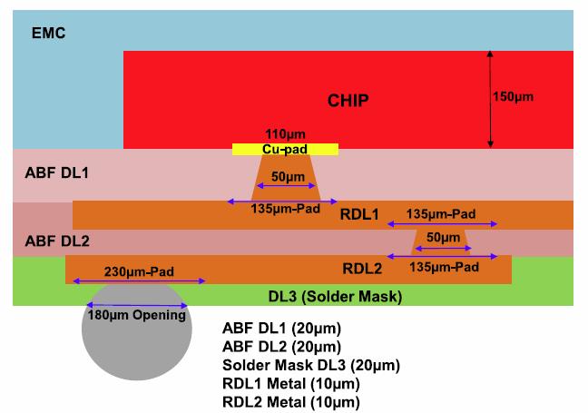
Figure 1. Cross-section of package build using the Uni-SIP process (image from reference [1])

In this case, a liquid epoxy mold compound from Nagase (R4507) was used in a modified compression molding process.  The EMC had high filler loading (85%) and a Tg of 150°C (DMA). The CTE below Tg was 10 ppm/K.  The redistribution layers were fabricated using Ajinomoto Build Up Films.

Figure 2 shows the attributes of the ABF type of RDL (courtesy of Ajinomoto Fine-Techno).  The ABF films are negative tone materials, that is they crosslink under UV exposure and thus the exposed area is rendered insoluble.  Recall that positive tone PBO and PI RDL dielectrics become soluble under UV exposure, the opposite of a negative tone resist.

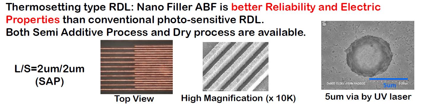
Figure 2. Characteristics of Ajinomoto Build Up Films used for redistribution layers in a panel level process (courtesy of Ajinomoto Fine-Techno).

In Figure 2, the optical photograph shows the ABF approach is capable of 2 µ lines and spaces and 5 µ diameter UV laser drilled vias.  The ABF dielectric layers are vacuum laminated onto the panel using printed circuit board methods.

The properties of the ABF layers are shown in the following table from reference [1].

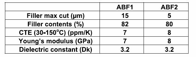
The Ajinomoto build-up film RDL layers are highly filled (80-82% loading) resulting in a low CTE in the range of 7-8 ppm/K.  Note that this is very close to the CTE of the Nagase R4507 epoxy mold compound.  The dielectric constant is important in the RDL since the signal speed will be impacted by the Df of the RDL layer.

A future post will cover the recent advances in build up films from both Ajinomoto and Sekisui.

References:

1 John Lau, et. al., Chip-First Fanout-Out Panel-Level Packaging for Heterogeneous Integration, IEEE Transaction on Components, Packaging and Manufacturing Technology, Vol. 8, No. 9, September 2018, p. 1561

Share on LinkedIn Share

Filed Under: Uncategorized

« Happy Thanksgiving
Polymers in Electronic Packaging: New Advances in Build-up Technology »

Leave a Reply

Your email address will not be published. Required fields are marked *

Polymer Innovation Blog

I’m Dr. Jeff Gotro and welcome to the Polymer Innovation Blog. Over the last 40 years I have been involved in polymer research, along with product and process development. I acquired invaluable experience working for IBM, AlliedSignal, Honeywell, Ablestik Labs (now Henkel) and in multiple consulting projects. In this blog, I (along with some guest contributors) will share our experiences, tips, and “tricks of the trade” to get more out of your innovation efforts and discuss new trends and technical advances in the polymer industry.
View Jeff Gotro, Ph.D., CMC's profile on LinkedIn

Innocentrix, LLC


Click to Visit Website

plastics expert witness
Click for More Information

Subscribe by Email

Search the Blog

Polymer Video Training

Visit our Video Store

Polymers in Electronic Packaging

polymers in electronic packaging Are you confused about what is electronic packaging? Have you ever wondered what type of polymers and polymer-based composites are used in electronics? Learn More...

Practical Tips for Curing Thermosets

practical tips for curing thermosets Have you ever had a question about the degree of cure or is your part fully cured after processing? Confused about what is gelation or how does vitrification impact thermoset curing? Learn More...

Rheology of Thermosets

rheology of thermosets Have you ever had a question about measuring the rheological properties of thermosets Didn’t know what is the right experimental approach to get the right rheological information? Learn More...

Dielectric Cure Monitoring of Thermosets

Dielectric Cure Monitoring of Thermosets Do you have a need for an in-situ cure monitor for a thermoset process but don’t know where to start? Are you confused about the terminology used in dielectric spectroscopy? Learn More...

Introduction to Biopolymers and Bioplastics

Introduction to Biopolymers and Bioplastics Would you like to know how sustainable are bio-based polymers? Or what is the market size and growth rate for bioplastics? Or have questions about the biomass supply chain? Learn More...

Thermoset Characterization

Thermoset Characterization Have you ever had a question about how to measure a physical property of a thermoset? Confused about what is gelation or how does vitrification impact thermoset curing profiles? Or wondered how to measure the glass transition temperature of an epoxy or polyester composite? Learn More...

Amazon.com Bookshelf

Robert's Rules of Innovation Thermal Analysis of Polymers Order

Copyright © 2025 Innocentrix, LLC · All Rights Reserved