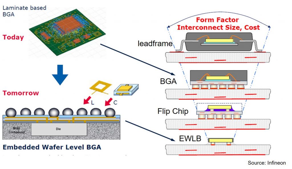
Figure 1. Technology progression leading to embedded wafer level BGA (or fan-out wafer level packaging)
In this series of posts, the technology progression for electronic packaging has been discussed. The first topic was leadframe packaging as seen on the top right in Figure 1. As the chip I/O (number of leads coming off the chip) increased, plastic ball grid array packaging addressed the requirement to connect the chip to the printed circuit board using a semiconductor substrate with an area array of solder balls on the backside. With increasing density, the next step in the packaging evolution was flip chip ball grid array (FCBGA). In FCBGA, the chip was solder bumped first and then attached face down, i.e. flipped over compared to previous packages. In all of these packages, polymers played an important role as die attach adhesives, epoxy mold compounds, underfills, and epoxy bismaleimide triazine substrate materials. Thermoset resins are the workhorse of electronic packaging.
The huge growth of the mobile phone industry is driving electronic packaging to new technologies. This post will provide an introduction to fan-out wafer level packaging (FO-WLP). The first embodiment of this new technology was introduced by Infineon and is shown in the lower left in Figure 1. Infineon called this revolutionary new package Embedded Wafer Level BGA (eWLB) since it eliminated the semiconductor substrate and embedded the redistribution wiring into the package. The eWLB was introduced in 2007 and jointly developed by Infineon, ST Microelectronics and STATS ChipPAC. After several years of development, FO-WLP in various configurations is shipping in high volume.
There are three process approaches used by various OSATS and foundries:
- Die first, face down
- Die first, face up
- Die last, face down
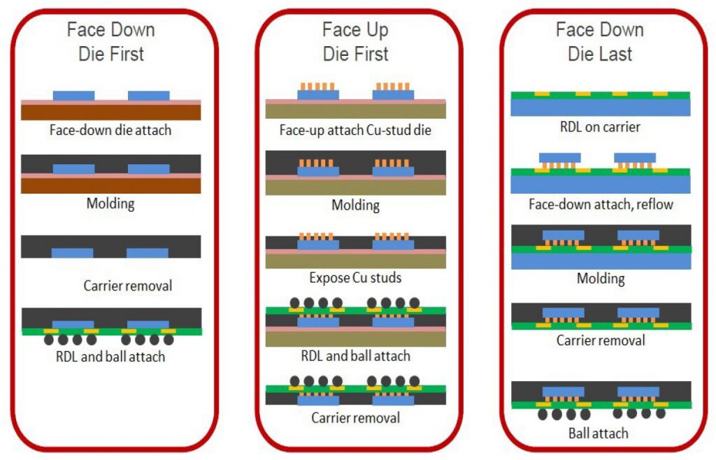
The process flows for each of the three approaches are shown in Figure 2.
Figure 2. Three approaches to fan-out wafer level packaging (source: SPIL)
The Infineon eWLB is the die first, face down process flow shown on the left in Figure 2. In Figure 2, only the high level process flow is shown. There are many very important and detailed processes involved at every step. In this case the known good die is attached to a carrier wafer using a temporary adhesive. The dies arranged on the carrier is called a reconstituted wafer. The next step is epoxy molding using a specially developed epoxy mold compound (EMC). The carrier is removed exposing the die face. Polymer redistribution layers (RDL) are added to the face of the die and in contact with the EMC. After several polymer dielectric application and lithographic steps, the multilayer RDL structure is completed. The next step is solder ball attach followed by singulation (cutting the finished packages out of the reconstituted wafer).
In the case of the die first, face up (middle image in Figure 2), the known good die is mounted face up on the temporary release adhesive/wafer carrier. Copper pillars are then plated on the active die surface. The next step involves encapsulation with EMC. After encapsulation, the top surface is ground down to expose the copper pillars. The next step entails adding layers of polymer RDL, photo-imaging vias and copper traces. The next step is solder ball attach followed by release from the carrier. The last step is singulation into the individual packages.
The face down, die last process is shown on the left in Figure 2. In this process flow, the RDL layers are formed on a carrier first. The face down, die last process has the advantage of testing the RDL structure and using known good RDL as well as attaching only known good die, thus increasing the yield. In the first two approaches (die first) if there is a problem with the RDL, there is a lot of value add that is scrap (EMC molding and RDL processing).
After the RDL structure is formed and tested, the chip is flip-chip attached onto the RDL supported on the carrier wafer. The flip-chips on RDL are then molded using EMC, followed by carrier removal, ball attach and singulation.
The next post will go into more process details.


Leave a Reply