Polymer Innovation Blog

Practical tips and advice for polymer, innovation and product development professionals

Polymer Innovation
  • Home
  • eBooks
    • Polymers in Electronic Packaging
    • Rheology of Thermosets eBook
    • Practical Tips for Curing Thermosets
    • Thermoset Characterization
    • Dielectric Cure Monitoring of Thermosets
    • Introduction to Biopolymers and Bioplastics
  • Videos
    • Core Curriculum: 3 Part Video Series
    • Characterization of Thermosets: 4 Part Video Series
    • Advanced Thermoset Cure Kinetics: 3 Part Video Series
    • DSC of Polymers: 5 Part Video Series
    • Thermoplastics: 5 Part Video Series
  • Services
    • Consulting
    • Polymer Expert Witness
  • Learning Center
    • White Paper
  • Why Jeff?
    • Speaker Info
  • Contact
  • Subscribe
  • Members
    • Login
    • Logout

Polymers in Electronic Packaging: Fan-Out Wafer Level Packaging Part Three

November 5, 2018 By Jeffrey Gotro 1 Comment

In this post we return to polymers in electronic packaging.  In October there were two electronic packaging conferences.  The International Microelectronics Assembly and Packaging Society (IMAPS) national conference was held in Pasadena, CA on October 8-11.  The second conference was the International Wafer Level Packaging Conference (IWLPC) which is held every year in San Jose.  This year the IWLPC was held on October 23-25.  The most exciting topics of discussion at both of these conferences was Fan-Out Wafer Level Packaging. Earlier in the year I had a couple introductory posts on Fan-Out Wafer Level Packaging [1, 2].

Let’s start with a quick update on the current status of wafer level packaging (WLP).  Wafer level packaging has transitioned from “powerpoint engineering” to volume production.  The key event in the explosion of eWLP was the announcement that Taiwan Semiconductor Manufacturing Corporation (TSMC) was going to package the Apple A10 processor using TSMC’s InFO (Integrated Fan Out).  The large impact of the TSMC entry is shown in Figure 1 (source: Yole Developpement).

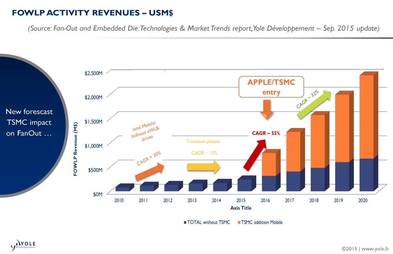
Figure 1. FOWLP revenues as a function of time (years)

Note in Figure 1 that the Apple share currently dominates the FOWLP production volumes from 2016 out to 2020.  While there is healthy growth for the rest of the FOWLP packagers (blue portion in Figure 1), the volumes are much smaller.  It should be noted this data is a bit dated, but I use it to demonstrate the market trends.

To review, the original FOWLP was developed to leverage the wafer fab equipment and processes.  The first FOWLP was done on circular 200 mm wafers, but quickly transitioned to 300 mm wafers to use the existing equipment set for that size wafer.  To date, most of the materials have been developed for 300 mm wafer processes (mold compounds, redistribution layers, temporary bonding adhesives).  A high level overview of the FOWLP process flow for 300 mm round wafers is shown in Figure 2.

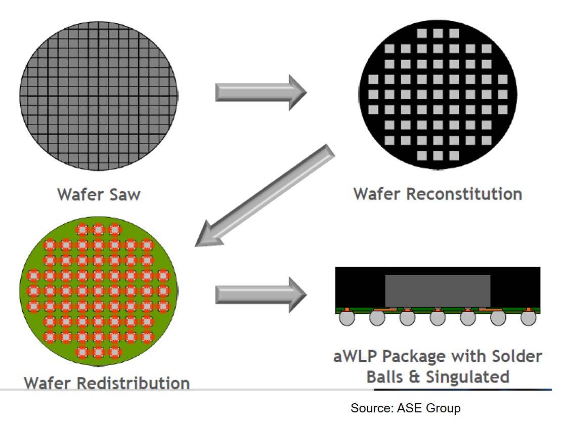
Figure 2. Fan-Out Wafer Level Process for 300 mm wafers (Source: ASE Group)

In anticipation of future volume ramps, many packagers started thinking about how to reduce cost.  For high-end chips (like the Apple A10 or A11) the wafer format will yield the best results in terms of yield and technology (smaller lines and spaces, more density, etc).  For low-end FOWLP such as used in mobile phones, cost will be an important driver.  In order to reduce cost, several packagers in the industry have started to evaluate making the FOWLP on a panel format.  The panel format is commonly used in the printed circuit board (PCB) and semiconductor substrate manufacturing process.  The typical panel size in the PCB industry is 18 inches X 24 inches.

Chet Palesko from SavanSys presented a paper at the 2014 IWLPC conference where he presented data on the cost structure of panel versus wafer.  His data indicated the following:

  • 300 mm wafer yields 616 10 mm x 10 mm packages
  • 400 mm x 500 mm panel yields 1,911 10 mm x 10 mm packages

To graphically illustrate the panel versus wafer production scale, AT&S (PCB producer, and thus used standard 18 x 24 inch panels) showed the following comparison in Figure 3.

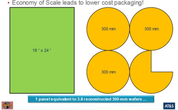
Figure 3. Panel versus wafer for FOWLP (Source: AT&S)

In Figure 3, one 18 x 24 inch panel is equivalent to 3.8 reconstituted 300 mm wafers which is similar to the 3.1 ratio SavanSys presented in the case of the 400 x 500 mm panel size (slightly smaller panel).  At the most recent electronic packaging conferences, there were panel discussions on “panels.”  While most of the details are closely held, there is consensus that at some point in the future (likely around 2020) panel formats will be widely available from several packagers.  On the other hand, TSMC will likely to continue to use the wafer format for the InFO process since it is integrated into the back end of the wafer fab process.

The next few posts will cover additional recent developments in the area of FOWLP.

References:

  1. https://polymerinnovationblog.com/polymers-in-electronic-packaging-introduction-to-fan-out-wafer-level-packaging/
  2. https://polymerinnovationblog.com/polymers-in-electronic-packaging-fan-out-wafer-level-packaging-part-two/
Share on LinkedIn Share

Filed Under: Uncategorized

« Thermoset Cure Kinetics Part 14: Analysis of Autocatalytic Systems from Conversion and Rate of Conversion Data
Remember Our Fallen Heroes on Veterans Day »

Leave a Reply

Your email address will not be published. Required fields are marked *

Polymer Innovation Blog

I’m Dr. Jeff Gotro and welcome to the Polymer Innovation Blog. Over the last 40 years I have been involved in polymer research, along with product and process development. I acquired invaluable experience working for IBM, AlliedSignal, Honeywell, Ablestik Labs (now Henkel) and in multiple consulting projects. In this blog, I (along with some guest contributors) will share our experiences, tips, and “tricks of the trade” to get more out of your innovation efforts and discuss new trends and technical advances in the polymer industry.
View Jeff Gotro, Ph.D., CMC's profile on LinkedIn

Innocentrix, LLC


Click to Visit Website

plastics expert witness
Click for More Information

Subscribe by Email

Search the Blog

Polymer Video Training

Visit our Video Store

Polymers in Electronic Packaging

polymers in electronic packaging Are you confused about what is electronic packaging? Have you ever wondered what type of polymers and polymer-based composites are used in electronics? Learn More...

Practical Tips for Curing Thermosets

practical tips for curing thermosets Have you ever had a question about the degree of cure or is your part fully cured after processing? Confused about what is gelation or how does vitrification impact thermoset curing? Learn More...

Rheology of Thermosets

rheology of thermosets Have you ever had a question about measuring the rheological properties of thermosets Didn’t know what is the right experimental approach to get the right rheological information? Learn More...

Dielectric Cure Monitoring of Thermosets

Dielectric Cure Monitoring of Thermosets Do you have a need for an in-situ cure monitor for a thermoset process but don’t know where to start? Are you confused about the terminology used in dielectric spectroscopy? Learn More...

Introduction to Biopolymers and Bioplastics

Introduction to Biopolymers and Bioplastics Would you like to know how sustainable are bio-based polymers? Or what is the market size and growth rate for bioplastics? Or have questions about the biomass supply chain? Learn More...

Thermoset Characterization

Thermoset Characterization Have you ever had a question about how to measure a physical property of a thermoset? Confused about what is gelation or how does vitrification impact thermoset curing profiles? Or wondered how to measure the glass transition temperature of an epoxy or polyester composite? Learn More...

Amazon.com Bookshelf

Robert's Rules of Innovation Thermal Analysis of Polymers Order

Copyright © 2025 Innocentrix, LLC · All Rights Reserved