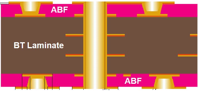
Figure 1. Cross section of a 1+4+1 HDI substrate using Ajinomoto build-up film (ABF)
The previous post discussed the geometry of the ABF products and the process used to build-up the circuit layers on the core. In Figure 1 above, there is one layer of ABF on each side of the 4 layer BT epoxy core. Notice in this schematic construction the plated through holes (PTH) extend from the top of the HDI substrate to the bottom. The vias in the ABF layers are laser drilled and the through holes are mechanically drilled. After both laser and mechanical drilling, the HDI substrate is prepared for copper plating in both types of interconnections. The laser drilled microvias and the through holes are typically cleaned using a desmear process to prep the via and through hole walls for copper seed and then copper plating. The desmear process removes the residual resin scum that may deposit on the bottom copper pad during laser drilling. Additionally, the desmear process cleans the copper pads that intersect the through hole to ensure good electrical connection to the copper layers in the core and the ABF.
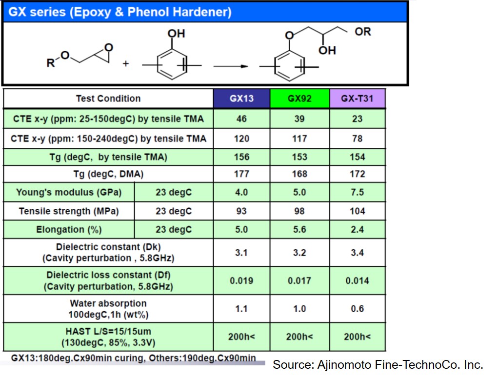
The first ABF products were the GX series and used epoxy resins with phenolic hardeners. The current Ajinomoto Fine-Techno Co., Inc. website (https://www.aft-website.com/en/electron/abf ) does not have any data for the GY series which used a phenolic ester hardener. The first ABF products were introduced in 1999 and have been continually improved as the packaging requirements became more demanding. The GX-13 product was introduced in 2005 and the GX-92 product was introduced in 2011. A recent addition to the epoxy ABF product line was the GX-T31. Table 1 shows the physical property, electrical and reliability data for the GX series.
Table 1. Properties of Ajinomoto Build-up Films (ABF) GX Series (source: Ajinomoto Fine-Techno Co. Inc.)
Table 1 shows several trends in the performance improvement from GX13 to GX-T31
- Lower coefficient of thermal expansion (CTE)
- Higher Young’s modulus
- Lower dielectric loss factor (Df)
- Lower water absorption (GX-T31 is almost 50% lower than GX13)
- Good reliability in biased HAST (highly accelerated stress testing)
An interesting observation is that the dielectric constant (Dk) slightly increases as the CTE is lowered indicating a slightly higher filler loading but the dielectric loss factor, Df progressively lowers as the ABF properties improved with time. The increased filler loading also increases the Young’s modulus and decreases the elongation percent (%). Interestingly, the Tg is not very different between the three epoxy-based ABF products potentially indicating the base epoxy-phenolic resin has not been significantly changed over time.
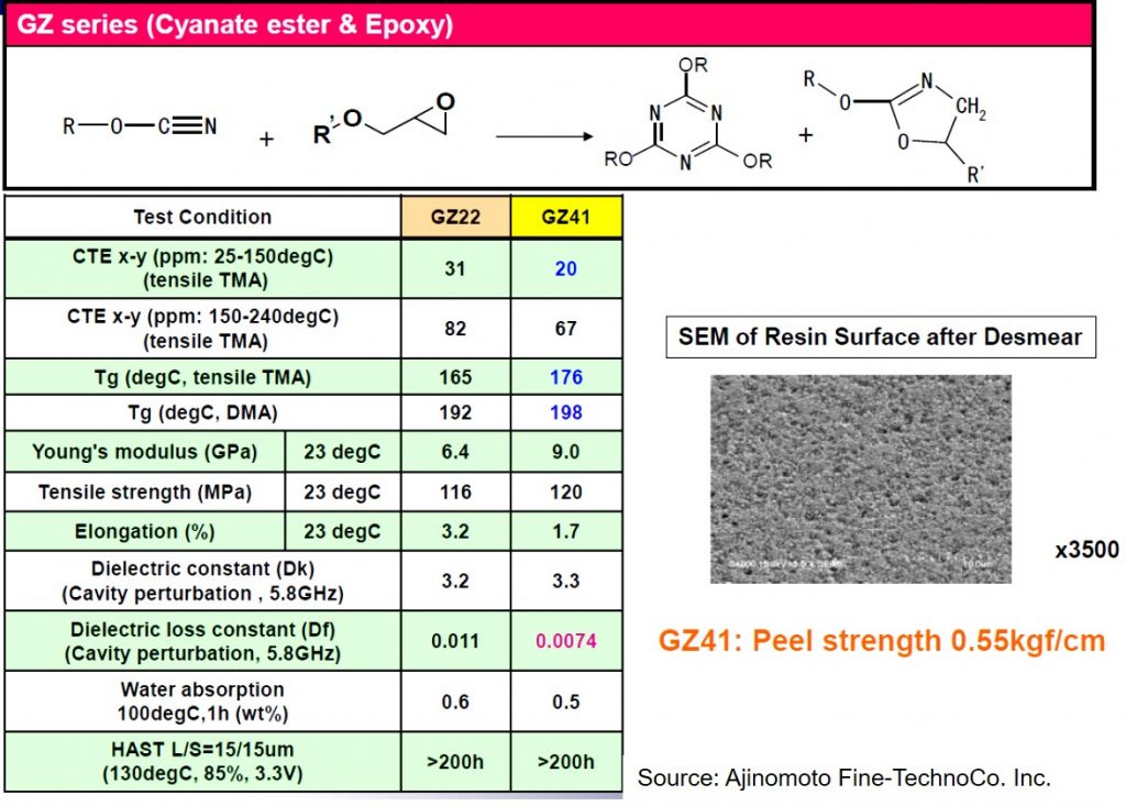
The drive towards faster signal speeds and lower loss has driven the development of a new series of ABF called the GZ series that incorporates cyanate ester into the base epoxy resin. Cyanate esters have low dielectric constants and more importantly low dielectric loss factors. Additionally, the use of cyanate esters with epoxy resins was first introduced by Mitsubishi Gas Chemical in the early 1980s with the BT-epoxy resins.
Table 2. Properties of Ajinomoto Build-up Films (ABF) GZ Series (source: Ajinomoto Fine-Techno Co. Inc.)
As shown in the chemical reaction scheme in Table 2, there are two main reaction products. The first is the cyclotrimerization of the cyanate esters into triazine ring structures. The triazine ring structures after polymerization have low polarity and thus have low Dk. The Df of the fully polymerized cyanate esters is also very low (Df is approximately 0.006 and Dk in the range of 2.6 at 1 GHz). GZ41 is currently listed on the Ajinomoto Fine-TechnoCo website (https://www.aft-website.com/en/electron/abf ). Th GZ41 has a very low dielectric loss factor but not a significantly lower Dk compared for example with GX-T31 in Table 1. The Tg and modulus of the epoxy cyanate ester system is higher than the GX-T31 indicating the stiffer nature of the triazine ring structures.
One should note that the reaction products of epoxy and cyanate ester during curing are very complex. In Table 2, the oxazoline ring structure (far right) is formed after the reaction of an epoxy with a cyanate group.
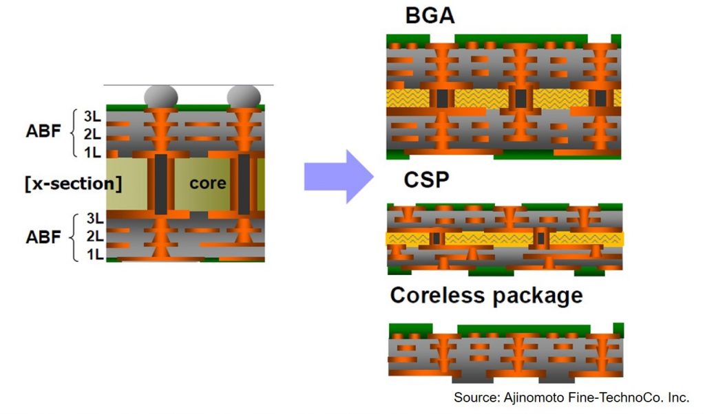
Figure 2 shows the build-up material roadmap starting with HDI circuit boards and progressing to coreless semiconductor packaging substrates.
Figure 2. Build-up material roadmap (source: Ajinomoto Fine-Techno Co. Inc.)
Figure 2 shows the evolution of build-up materials. What is interesting to note is the trend to thinner BT-epoxy cores and eventually to a coreless package. The schematic in the top right image depicts a very high density ball grid array (BGA) semiconductor substrate, most likely used for high density flip chip applications (FC-BGA). As the substrate gets thinner (by reducing the core thickness and thinner build-up layers), chip scale packages (CSP) are enabled. In a CSP, the substrate area is approximately 20% larger than the area of the semiconductor chip [1].
Future requirements for build-up materials:
- Fine line and space
- High adhesion strength with low copper surface roughness
- Fine via pitch
- Low warpage during cure and reflow (requires low CTE)
- Low dielectric constant and loss factor for improved electrical performance
The next post will go into the details of the manufacturing process for ABF and introduce the concept of a Resin Coated Copper (RCC) build-up film.
References
Jeff, Enjoyed reading your blog on BU substrate. Are there any development beyond GZ41 that addresses the mechanical properties requirement along with further low loss property? Again, your blog is very informative..
wondering if you see a need for high temperature board materials such as cyanate ester and Bismaliemide?
Bismaleimides have been used for over 40 years in the Mitsubishi Gas Chemical BT epoxy resin used in semiconductor substrates. BTW, the B in BT is bismaleimide and the T is triazine (or cyanate ester). Additionally, some cyanate esters and blends have been used in high-end specialty substrates/laminates.