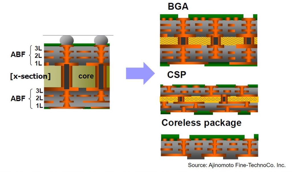
Figure 1. Build-up material roadmap (source: Ajinomoto Fine-Techno Co. Inc.)
The last post described the chemistry and types of build-up films typically used in the electronic packaging industry. We also touched on the build-up material roadmap which showed the various complex packaging substrates that are enabled using build-up film technology as shown in Figure 1. During my writing for the last posts on build-up film technology, I came across a great presentation titled Low Df Build-up Material for High Frequency Signal Transmission Substrates, by Hirohisa Harahashi, Ajinomoto presented at the Electronic Components and Technology Conference (ECTC), May 2013 (Cosmopolitan Hotel). Click here to view. I will discuss some of the polymer related issues in the build-up film technology in this post.
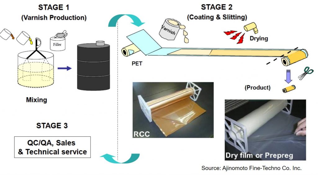
Figure 2. Process to fabricate Ajinomoto build up films (ABF) and resin coated copper (ABF-RCC)
The ABF process starts with the compounding of the varnish which consists of the resins (epoxy, cyanate esters), hardeners and fillers. The exact chemical composition of the resins, hardeners and fillers is not disclosed. From some of the micrographs in the ECTC presentation, there is a fairly high filler loading. The resin system is termed a “pre-mixed one-part” type of chemistry since the resin and hardener are both added during the compounding step. To have room temperature shelf life (and work life on the manufacturing floor), the curing chemistry will need high temperature to initiate the curing reactions. Typical curing schedules for the ABF films require 180 – 190°C for 90 minutes.
Once the varnish is compounded, the liquid is coated only a 38 µm PET support film and dried. It was not disclosed whether a solvent is used and the temperature profile. There are two potential ways to make the build-up film. One is to simple evaporate the solvent during the drying process and then apply the polypropylene cover film. If oligomers with higher molecular weights and high filler loadings are used, then the material may have film-like properties after drying. The second scenario would involve both drying and subsequent B-staging to obtain the film-like properties. In any case, the build-up films will have sufficient strength to be able to be wound onto mandrels and shipped to the customer. The resin coating layer thickness ranges from 10-100 µm.
One of the driving forces to use ABF resin coated copper was to enable the use of fine copper films. Traditional copper foils have a distinct nodule structure on the backside to enhance adhesion but limit both the lines/spaces and the electrical transmission speed. Low profile (smooth) copper enables fine lines and spaces (down to 5 µm lines/spaces) and increases the electrical signal speed.
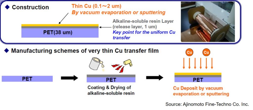
Figure 3 shows the ABF-RCC construction.
Figure 3. Very thin copper transfer film with ABF (source: Ajinomoto Fine-Techno Co. Inc.)
The ABF-RCC consists of a three layer structure; 38 µm PET support film, an alkaline-soluble resin release layer, and a very thin vacuum evaporated copper layer (0.1 – 2 µm). Similar to the coating process for standard ABF, the alkaline-soluble release layer is coated onto the PET carrier and dried. In the next step, the very thin copper is deposited by vacuum evaporation or sputtering. The next step is to laminate the thin copper layer onto the ABF layer as shown in Figure 4.
Figure 4. Process to manufacture ABF-RCC (source: Ajinomoto Fine-Techno Co. Inc.)
In contrast to the standard ABF products (GX and GZ series) the ABF-RCC has a very thin layer of copper attached to the release layer. The manufacturing process to build the HDI layers is shown in Figure 5.
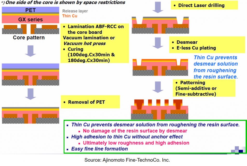
Figure 5. Detailed process flow to fabricate build-up layers using ABF resin coated copper (RCC) (Note: process flow shows only one side. In production the ABF RCC would be applied to both sides) (source: Ajinomoto Fine-Techno Co. Inc.)
The process begins by removing the PET carrier in contact with the ABF resin. The next step is the vacuum lamination of the ABF to the circuitized core. The ABF resin will soften and flow wetting the core surface and filling the gaps between the circuit traces and more importantly, completely filling the vias or through holes (if required). The curing process involves a two-step cure; the first step at 100°C is used to soften and flow the ABF to ensure good coverage and filling while not causing the crosslinking reaction to occur at an appreciable rate. The subsequent 180°C hold for 30 minutes is designed to fully cure the ABF film. Note that in this case the 180°C temperature is above the ultimate glass transition temperature (Tg for the GX series is 168-177°C by DMA). From our previous posts, we stressed how important the curing temperature be higher than the ultimate Tg to prevent vitrification from occurring during the cure process.
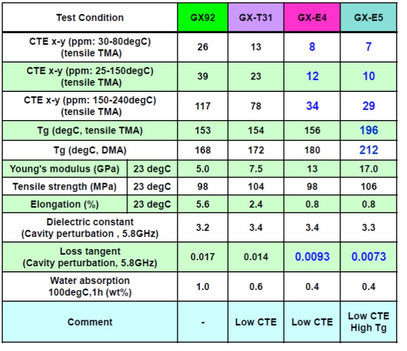
After lamination, the PET carrier is removed and the vias are formed using laser drilling with CO2 or UV-YAG laser drills. The importance of the thin copper is now evident in that the laser drilling process must penetrate through the very thin copper layer in order to form the vias. An additional note is that the fillers in the build-up films will also make it harder to laser drill. The laser drilling process and careful attention to the details of the fillers will result in acceptable via structures. The rest of the circuit and via forming process using standard plating and photolithography is shown on the right side of Figure 5. The properties of the ABF-RCC films are shown in Table 1 and are designated as GX-E4 and GX-E5.
Table 1. ABF GX Series with Thin Copper Transfer Film (source: Ajinomoto Fine-Techno Co. Inc.)

Please send me Technology Roadmap the covers the ABF film.