
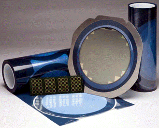
 Source: Henkel
The last post described the dicing die attach film (DDAF) approach used in multiple die stacking. This post will discuss the application of DDAF and some of the interesting aspects of using the “bundled” die attach film on the dicing tape. In Figure 1, the die attach and stacking process is shown for a two-die stack. The process begins with the placement of the first layer of die attach adhesive onto the plastic ball grid array (PBGA) substrate. In the early generations of die stacking, a paste die attach was used to fill in the topography of the lines and pads on the surface of the PBGA substrate. Soldermask was used to protect the PBGA circuit traces and open the pads on the surface to enable wire bonding. The soldermask placed over the circuit lines resulted in an uneven surface and die attach paste was initially used since it was easy to flow and fill-in the uneven surface. Later generations of DDAF had more flow and was also able to fill and planarized the PBGA surface.
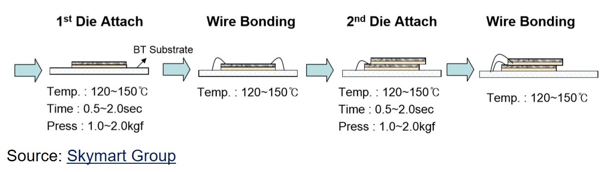
Figure 1. Die Stacking Process
In the figure above, the PBGA substrate is depicted using a bismaleimide triazine (BT) substrate. When using DDAF, recall the die attach film is attached to the die backside and during the first die attach, the film die attach softens and flows. Note the temperature and pressures are optimized for the particular type of die attach film being used. The DDAF is B-staged so it has film-like properties during the pick-and-place operation, but at the bonding temperatures can soften and flow. The DDAF film must have enough tack or adhesion to be able to be wire bonded in the next step. After wirebonding, the second die is attached to the top surface of the mother (bottom) die. After the second die is attached, the second wirebonding to the daughter (second) die is completed. Not shown in Figure 1 is the epoxy molding process. After all of the wire bonding is completed, the entire die stack is over molded using epoxy mold compound (EMC).
In Figure 2, the die stacking technology progression is shown.
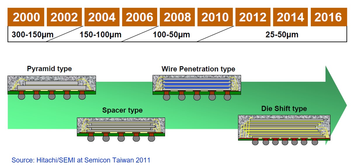
Figure 2. Die stacking technology progression
In Figure 2, the die attach film thickness is shown for several date ranges. Notice the progressive thinning of the bondline thickness over time. The bondline thickness reduction was the main driver for the use of DDAF. The first die stacking approach was called the pyramid type where the daughter die was smaller than the mother die. Many of these early applications used paste die attach. The transition to film die attach occurred with the need for same-die stacking.
The first generation of die attach film for same-die stacking used film adhesives and a spacer. The spacer was required to prevent the daughter die (second chip) from damaging the wire loop coming off the mother die (first die attached to the substrate). In Figure 2, see the red dashed circle on the right side of the schematic.
![]()
Figure 3. Spacer die stacking approach
In Figure 3, the spacer also had to have a thin layer of die attach film (not shown) and involved an extra step of placing the spacer. The next generation of die attach film was developed to eliminate the spacers and was called Flow Over Wire (FOW) as seen in Figure 4.
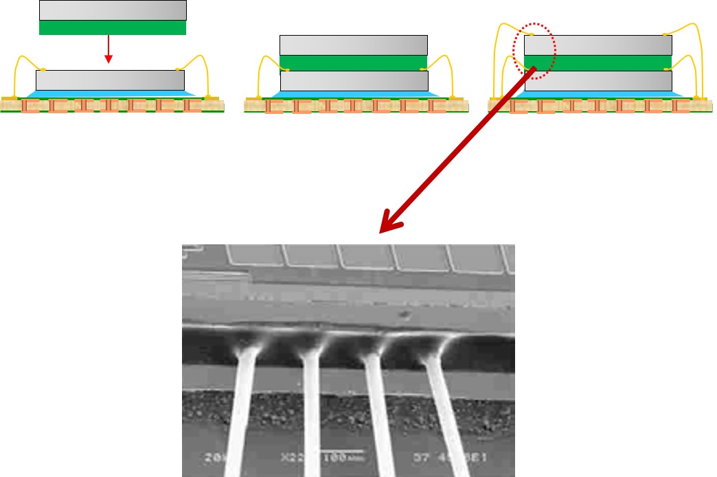
Figure 4. Flow Over Wire (FOW) die stacking approach
In Figure 4, the FOW die attach film is pick-and-placed in the die stacking operation as in the previous generations, but the DDAF has been modified to allow the film adhesive to flow around the wires allowing same-die stacking (middle and right stacks in Figure 4).
The flow over wire (FOW) film properties:
- Rheological properties are modified to allow the resin to flow over and encapsulate the wires
- Same base chemistries used, but formulations are optimized for proper B-stage and subsequent flow
- Chemical modifiers are added to enhance wetting of the copper or gold wirebonds
This is another great example of the utility of thermoset polymers in electronic packaging. The ability to precisely control the B-stage allows a tack-free film to be coated onto the dicing tape, but since the film is only partially cured, upon application of heat and pressure during the pick-and-place operation, the die attach film will soften, wet the top of the daughter die and flow around the wires. The viscosity at the B-stage is critical to get enough flow, but not too much flow causing the top die to damage the wirebonds. Another great example of thermoset chemistry in action.
Leave a Reply