
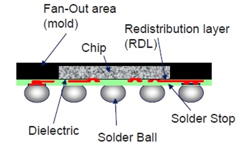
 This post will describe the use of a photosensitive positive-tone dielectric based on polybenzoxazole (PBO) used as the redistribution layers (RDL) in Fan-Out Wafer Level Packaging (FOWLP). To meet the challenges for FOWLP, such as lower curing temperatures (compared with polyimides that cure at over 300°C), low modulus, high elongation, and good electrical insulation, HD Microsystems developed a photosensitive PBO called HD 8940 (1-2) that can be cured at 200°C.
In Figure 1, the process flow for one dielectric layer is shown.
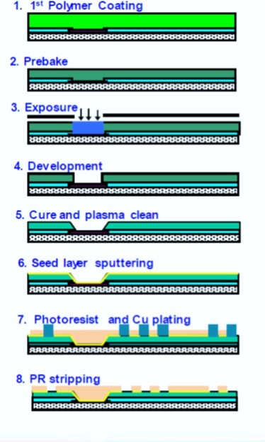
Figure 1. Process flow for forming a single dielectric layer in a FOWLP (image courtesy of JSR).
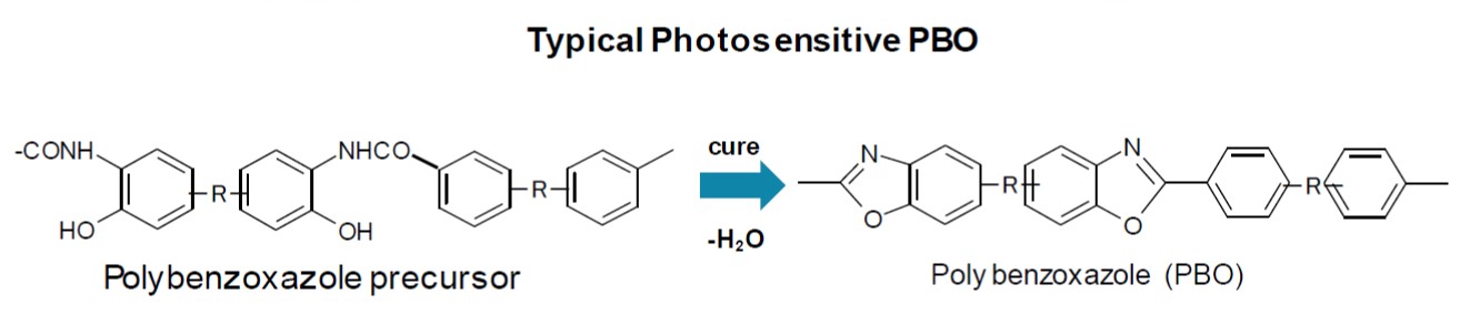
In step 1, the HD 8940 is spin coated on the top of the reconstituted wafer. In step 2, the HD 8940 is pre-baked at 120°C for 3 minutes. The positive-tone photosensitive PBO was patterned and exposed with a high-pressure mercury lamp at 230 mJ/cm2 forming the latent image in the dielectric layer. In step 4, the latent image was developed using the aqueous developer tetramethylammonium hydroxide (TMAH) forming vias and circuit traces in the dielectric material. In step 5, the PBO was cured at 200°C for 1 hour. During the curing process, the PBO cures by ring closure resulting in a high Tg, tough dielectric layer.
After curing, the dielectric thickness is in the range of 5-10 microns depending on the specific FOWLP structure. The subsequent circuitization processes such as seed layer plating, photoresist application, copper plating, and resist stripping are shown steps 6-8 in Figure 1.
Table 1 shows the typical properties of four types of dielectric layers; HD-4100 negative-tone photosensitive polyimide (PSPI), HD-8820 positive-tone PBO, HD-8930, positive-tone PBO, and HD-8840, positive-tone PBO (2).
TABLE 1 (from reference 2)
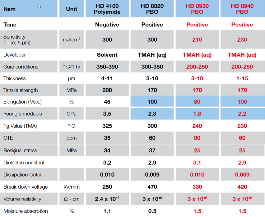
In Table 1, we will focus our discussion on the low temperature curing (in red) PBO dielectric layers and more specifically HD-8940. For HD-8930 and HD-8940, listed in Table 1, the cure temperature was 200°C indicating success in formulating the PBO to have a much lower cure temperature compared to the PSPI. In Table 1, the percent elongation maximum (%) and the Young’s modulus data are highlighted in light blue. For stress control in the dielectric layer, lower modulus and higher elongation to break are required. In the case of HD-8940, the percent elongation is over twice the % elongation for the polyimide HD-4100 and equal to the percent elongation for PBO HD-8820. The Young’s modulus for HD-8940 is approximately 60% lower compared with HD-4100 PSPI and nearly the same as HD-8820 PBO. The mechanical properties were able to be maintained for both of the lower cure temperature (200°C) polybenzoxazole dielectrics. One area for concern is the high coefficient of thermal expansion (CTE) of the PBO dielectrics, in the range of 60-80 ppm/°C. The epoxy mold compound (EMC) for FOWLP is formulated to have a very low CTE, in the range of 7-10 ppm/°C below Tg and 26-40 ppm/°C above Tg. The CTE mismatch between the EMC and the dielectric layer may result in stresses at the interface and potential loss of adhesion. Nishimura and Toba (reference 1) studied the adhesion of HD8940 to EMC as a function of time in the pressure cooker test (PCT) and found the shear adhesion of the PBO to the EMC to be unchanged up to 500 hours of testing.
The glass transition temperature (Tg) for the HD-8940 is 230°C. The HD-8940 is also a good dielectric insulator with a 2.9 dielectric constant and a low 0.009 dissipation factor. The combination of low curing temperatures (more compatible with the epoxy mold compounds), the higher percent elongation (better toughness) and lower modulus (lower residual stresses) makes HD-8940 a good candidate for FOWLP applications.
References
- Nishimura and M. Toba, “Evaluation of Fan-Out Wafer Level Package Using 200C Curable Positive-Tone Photodefineable Polybenzoxazoles,” CPMT Symposioum, Japan ((ICSS) 1025, IEEE, P. 25-28
- Polyimide and polybenzoxazole technology for wafer-level packaging, Chad Roberts, HD Microsystems, Chip Scale Review, July-August, 2015 p. 26-31.
Leave a Reply