
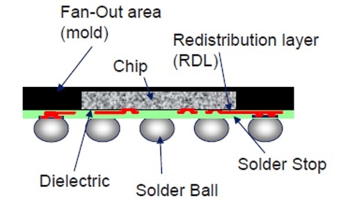
 The last post focused on molding compounds used in Fan-Out Wafer Level Packaging (FOWLP) as seen in black in the image above (source Infineon). A key enabler in the fan-out package is the polymer redistribution layer (RDL) or sometimes referred to as the dielectric layer. There are several types of polymers used as photosensitive dielectrics in FOWLP:
- Polyimide (PI)
- Polybenzoxazole (PBO)
- Benzocylobutene (BCB)
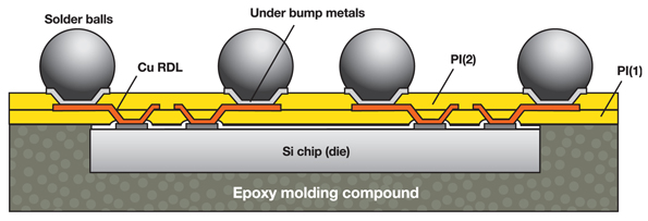
Figure 1. Two layer RDL in Fan-out Wafer Level Packaging
In Figure 1, two layers of the redistribution layer are shown in yellow (PI(1) and PI(2)). The red lines represent copper circuit traces (Cu RDL) and vias to enable layer-to-layer interconnections and “fan-out” the electrical circuits using the top surface of the chip and the surface of the mold compound. Adhesion of the dielectric layer to the epoxy mold compound is critical to achieve high level of reliability. In most types of electronic packaging, the metal (in this case copper) traces are formed by a combination of photolithography and plating. To fabricate the lines and vias, a photosensitive material called a photoresist is used. A schematic of the photoresist process is shown in Figure 2.
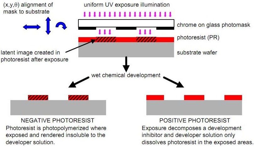
Figure 2. Schematic of the photoresist process used to produce circuit traces and vias.
The photoresist (PR) is applied to the substrate and in the case of FOWLP, the top side of the reconstituted wafer as seen in Figure 1. The next step is to place a photomask over the photoresist and align carefully so the features are in the right location after the photolithography process. Typically, optical registration tools are used to ensure the mask is in the proper X, Y and Z locations and also placed parallel to the photoresist surface. As shown in Figure 2, the photomask is used to let the UV light hit the photoresist the exposed areas forming a latent image.
There are two types of photoresists; negative and positive. In the case of a negative type photoresist, the area exposed to the UV light undergoes a chemical reaction to increase the molecular weight. The areas not exposed to the UV light remain essentially unreacted. The difference in the molecular weights between the exposed and unexposed photoresist causes a differential solubility in the developer. The developer is a solvent that removes the unexposed photoresist leaving the exposed regions on the part. The UV exposure renders the exposed areas insoluble in the developer solution.
For a positive tone photoresist, the UV exposure results in photoresist decomposition and the developer solution only dissolves the photoresist in the exposed areas. The photomask therefore will have either a negative or a positive image of the features required after development. For fine lines and spaces, positive tone resists are typically used. For the FOWLP process, a high level representation of the photolithography process used to form the RDL layers is shown in Figure 3.
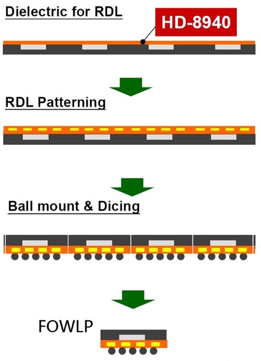
Figure 3. Schematic of the RDL process, ball mounting and dicing for FOWLP (Image: Hitachi)
The first step in the RDL process is to apply the photoresist to the reconstituted wafer using spin coating (easy to spin coat since the reconstituted wafer is circular). In Figure 3, HD Microsystems HD-8940 is a positive tone photoresist using a low temperature curing polybenzoxazole (PBO). The next step involved pattering the photoresist (multiple steps) and plating layer one. After the first lithography and plating steps are completed, a second layer of the photosensitive dielectric is applied and the process repeated to form the second RDL.
The next post will provide a more detailed discussion of the photolithography process and the use of PBO’s for FOWLP.
Leave a Reply