
 The last post discussed leadframe packages that were some of the first semiconductor packaging approaches. As the need for higher chip I/O, leadframe packages with more leads were developed. To increase the lead count, leadframes were developed to have the leads on all four sides of the molded package. These were termed Quad Flat Packs (QFP) since the leads came off all four sides of the package. An example is shown in the image on the above (source: Atmel). Notice that the leads now have “feet” on them. As the packaging density increased, the molded packages were now soldered to pads on the circuit board in a process called surface mount. Over time the lead count continued to increase and the molded leadframe packages became thinner. The higher lead count, thinner package was called a TQFP or thin quad flat pack. The next generation of leadframe packages was a QFN, of quad flat pack, no lead. The QFN package reduced the footprint of the package by have the surface mount leads on the bottom edges of the molded package as can be seen in the following image.
Figure 1. Quad Flat Pack, No Lead (QFN) package (source: Infineon)
The key feature in the QFN package is the lack of the “feet” thereby reducing the space required on the printed circuit board. Additionally, the die pad is exposed (center) allowing for better heat transfer out of the package. A typical QFN cross-section is shown in Figure 2.
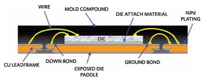
Figure 2. Cross-section of QFN package (source: Maxim)
The main polymeric materials used in the QFN package is the same as the previous leadframe packages, namely die attach adhesive and epoxy mold compound. In the case of the QFN, a die attach adhesive with enhanced thermal conductivity would make the package more thermally efficient. In Figure 2, the QFN was sawed from a part containing multiple wirebonded dies. Note the square edges at both the leadframe pads and in the mold compound. Some QFN’s are molded individually and are punched from the leadframe. In either case the cross-section is essentially the same.
Figure 3 (from reference [1]) nicely shows the progression from dual in-line IC packages, to QFP, chip scale package (such as the QFN) and then to the plastic ball grid array (PBGA).
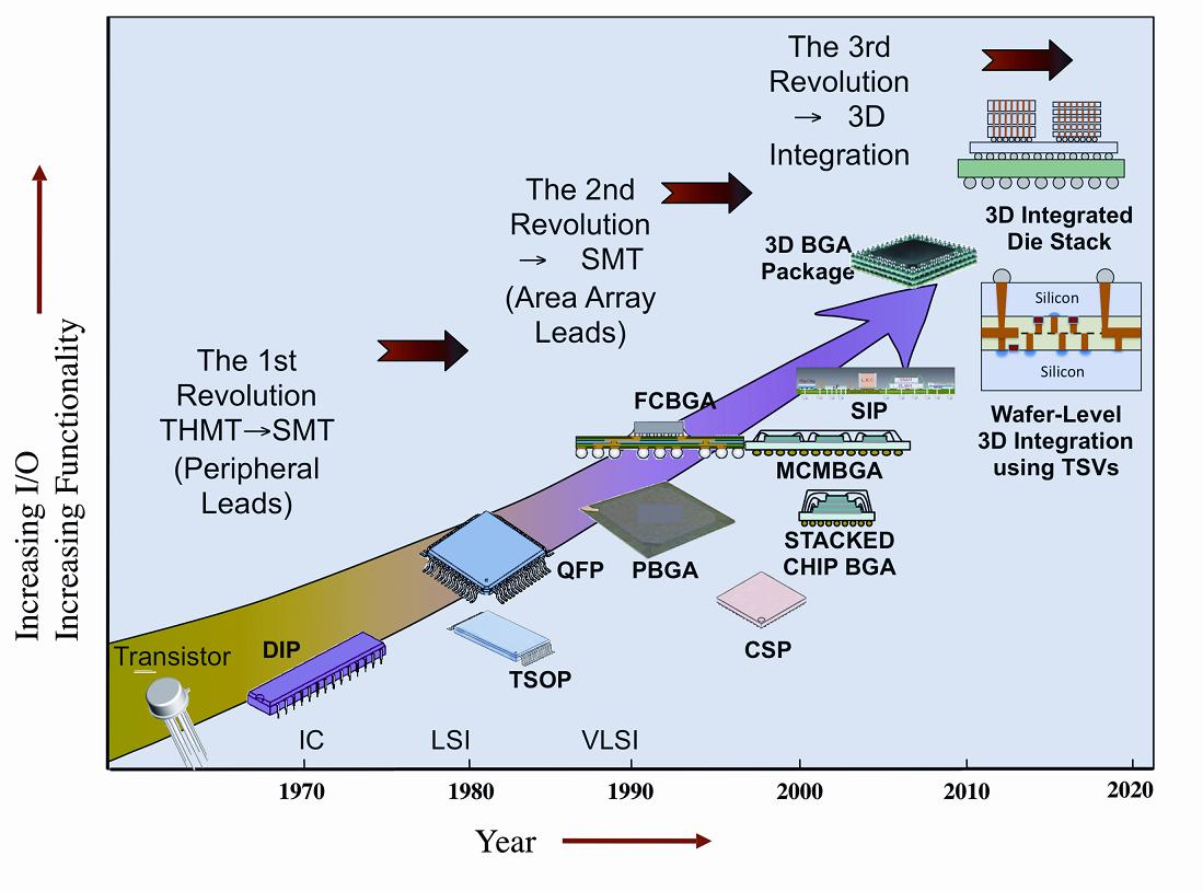
Figure 3. Packaging Evolution as a Function of Time (reference [1])
The chart shows the timing for some of the major shifts in packaging technology. As discussed, the original DIP’s were through hole mounted during the timeframe of the 60’s to 1970’s (THMT in Figure 3). In the 1980’s there was a transition to surface mount (SMT) components and the leading-edge package was the QFP. All of these packages used die attach adhesive, gold wire bonds connected the chip to the leadframe, and were encapsulated using epoxy mold compounds (EMC). Around 1990, a completely new type of package was developed called the plastic ball grid array (PBGA). Instead of using a leadframe, a laminate substrate was used and the PBGA substrate did not have peripheral leads, but rather the substrate was used to “fanout” the chip I/O to an area array on the back side of the laminate. Figure 4 shows several types of PBGA packages.
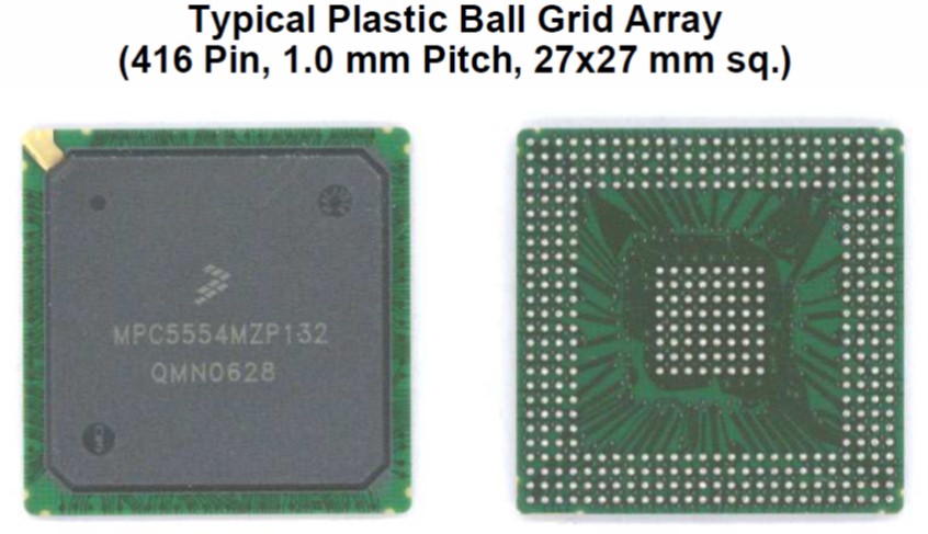
Figure 4. Example of a plastic ball grid array (PBGA) type package (source: NXP Freescale).
The PBGA package is capable of a much larger number of chip connections (I/O’s) and the purpose of the laminate substrate is to take the wirebonds on the top side of the laminate and route through the laminate substrate to solder balls on the back side. Since the solder balls are arranged in a pattern called an area array, to maximize the number of chip connections that can be made to the printed circuit board. The next post will describe in more detail the plastic ball grid array package.
References:
Leave a Reply