Polymer Innovation Blog

Practical tips and advice for polymer, innovation and product development professionals

Polymer Innovation
  • Home
  • eBooks
    • Polymers in Electronic Packaging
    • Rheology of Thermosets eBook
    • Practical Tips for Curing Thermosets
    • Thermoset Characterization
    • Dielectric Cure Monitoring of Thermosets
    • Introduction to Biopolymers and Bioplastics
  • Videos
    • Core Curriculum: 3 Part Video Series
    • Characterization of Thermosets: 4 Part Video Series
    • Advanced Thermoset Cure Kinetics: 3 Part Video Series
    • DSC of Polymers: 5 Part Video Series
    • Thermoplastics: 5 Part Video Series
  • Services
    • Consulting
    • Polymer Expert Witness
  • Learning Center
    • White Paper
  • Why Jeff?
    • Speaker Info
  • Contact
  • Subscribe
  • Members
    • Login
    • Logout

Polymers in Electronic Packaging: Wire Bonded Packages

February 5, 2018 By Jeffrey Gotro Leave a Comment

With the thermoset basics behind us, the next series of posts will discuss the various types of electronic packages.  There is a very specific lexicon in the electronic packaging industry and it would help the reader to first get an understanding of the rationale for the various packaging types and then provide a detailed discussion around the polymers used in these packages.  In Figure 1, the packaging evolution is shown.

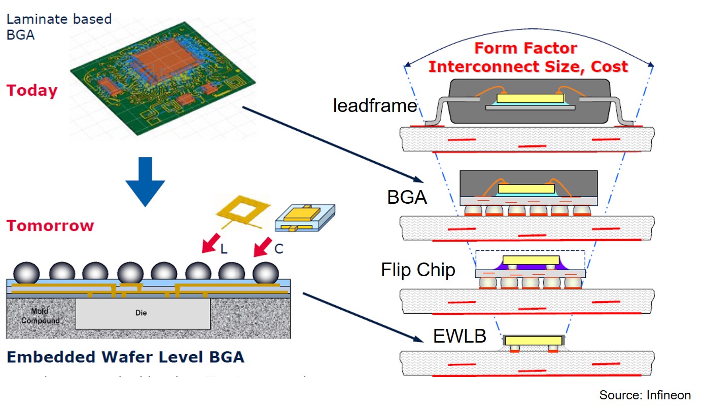
Figure 1. Schematic of electronic packaging types (Source: Infineon)

This is a great figure to “set the table” for the subsequent discussions of polymers in electronic packaging.  For now, let’s focus on the technology progression on the right side of Figure 1.  The yellow rectangles represent the semiconductor chips.  The term “semiconductor package” arose since the semiconductor chip or “die” must be connected via electrical connections to the base circuit board.  The term “die” results from the fact that semiconductor chips are made on circular wafers and after fabrication they are cut from the wafer using a wafer saw in a process called “dicing.”  In the electronic packaging lexicon, the terms chip and die are used interchangeably.

The first type of semiconductor package was the leadframe package as seen on the top right in Figure 1.  The yellow rectangle is the semiconductor die and the teal material is the die attach adhesive.  The die and die attach are place on the leadframe die pad (grey) and the top of the chip is attached to the lead fingers using either gold or copper wire bonds (orange).  The lead fingers are then soldered onto the printed circuit board.  If you have ever looked at the main circuit board inside you desktop PC, you will see a lot of black packages with little feet (leadfingers) soldered to the mother board.

The first leadframe package was called a “dual in-line” package or DIP.  The lead fingers consisted of two rows of leadfingers initially soldered into plated through holes on the circuit board and later the leadfingers were surface mounted.  An example of the metal leadframe is shown in Figure 2.

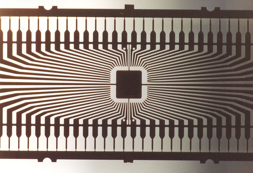
Figure 2. Metal leadframe (source: Motorola Reference [1])

The square in the center is the die attach pad where the die attach adhesive will first be dispensed and then the semiconductor chip will be placed on the die attach adhesive.  The metal leadframe can be copper, copper plated with silver (most common), or a pre-plated leadframe (copper base with nickel and palladium plating layers with a thin flash gold plated surface layer).  Wirebonding is the process by which small gold or copper wire is attached from the bond pad on the top of the chip to one of the leadfingers around the die pad.  A schematic of the cross section for a dual in-line package is shown in Figure 3.

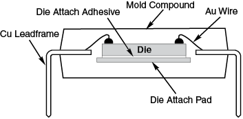
Figure 3. Schematic of dual in-line (DIP) package

After the wirebonding process, the leadframe, wires, and part of the leadfingers are over-molded using epoxy mold compound (EMC).  The purpose of the EMC is to protect the semiconductor chip from mechanical damage and reduce moisture diffusion into the package and damage the chip.  An image of a molded DIP is shown in Figure 4.

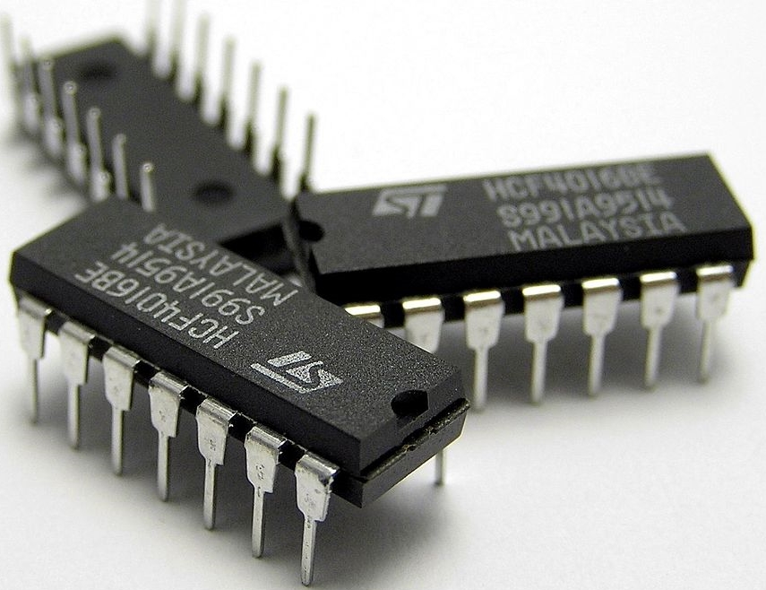
Figure 4. Finished dual in-line package (DIP) (from ST Microelectronics)

The DIP in Figure 4 is an example of a very simple DIP package (only 14 leads) but shows what the final molded part will look like.  The epoxy mold compound is a highly filled thermoset, typically an epoxy cresol novolac cured with a phenolic curing agent.  For more information see references 2 and 3.

Subsequent posts will discuss Ball Grid Array (BGA) packages, flip chip packages, and Fan Out Wafer Level Packages.

References

  • Leadframe image
  • Introduction to epoxy mold compounds
  • Epoxy mold compounds
Share on LinkedIn Share

Filed Under: Uncategorized

« Polymers in Electronic Packaging: Thermoset Network Formation
Polymers in Electronic Packaging: Wire Bonded Packages »

Leave a Reply

Your email address will not be published. Required fields are marked *

Polymer Innovation Blog

I’m Dr. Jeff Gotro and welcome to the Polymer Innovation Blog. Over the last 40 years I have been involved in polymer research, along with product and process development. I acquired invaluable experience working for IBM, AlliedSignal, Honeywell, Ablestik Labs (now Henkel) and in multiple consulting projects. In this blog, I (along with some guest contributors) will share our experiences, tips, and “tricks of the trade” to get more out of your innovation efforts and discuss new trends and technical advances in the polymer industry.
View Jeff Gotro, Ph.D., CMC's profile on LinkedIn

Innocentrix, LLC


Click to Visit Website

plastics expert witness
Click for More Information

Subscribe by Email

Search the Blog

Polymer Video Training

Visit our Video Store

Polymers in Electronic Packaging

polymers in electronic packaging Are you confused about what is electronic packaging? Have you ever wondered what type of polymers and polymer-based composites are used in electronics? Learn More...

Practical Tips for Curing Thermosets

practical tips for curing thermosets Have you ever had a question about the degree of cure or is your part fully cured after processing? Confused about what is gelation or how does vitrification impact thermoset curing? Learn More...

Rheology of Thermosets

rheology of thermosets Have you ever had a question about measuring the rheological properties of thermosets Didn’t know what is the right experimental approach to get the right rheological information? Learn More...

Dielectric Cure Monitoring of Thermosets

Dielectric Cure Monitoring of Thermosets Do you have a need for an in-situ cure monitor for a thermoset process but don’t know where to start? Are you confused about the terminology used in dielectric spectroscopy? Learn More...

Introduction to Biopolymers and Bioplastics

Introduction to Biopolymers and Bioplastics Would you like to know how sustainable are bio-based polymers? Or what is the market size and growth rate for bioplastics? Or have questions about the biomass supply chain? Learn More...

Thermoset Characterization

Thermoset Characterization Have you ever had a question about how to measure a physical property of a thermoset? Confused about what is gelation or how does vitrification impact thermoset curing profiles? Or wondered how to measure the glass transition temperature of an epoxy or polyester composite? Learn More...

Amazon.com Bookshelf

Robert's Rules of Innovation Thermal Analysis of Polymers Order

Copyright © 2025 Innocentrix, LLC · All Rights Reserved