
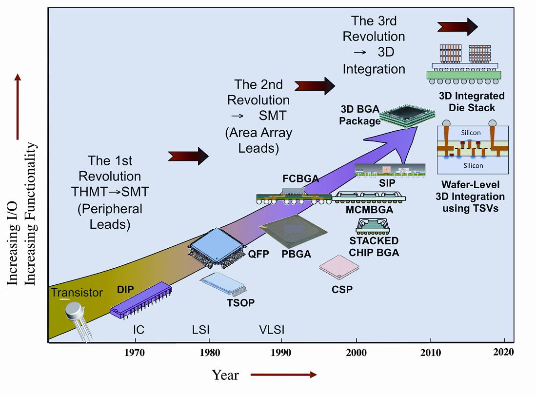
 The last post discussed advanced leadframe packages such as the QFP and QFN and introduced the plastic ball grid array (PBGA). The second major change in packaging technology occurred in the 1990’s when surface mount technology (SMT) was displaced by area array packages to achieve higher I/O density. This post focuses on the details of the plastic ball grid array package (PBGA).
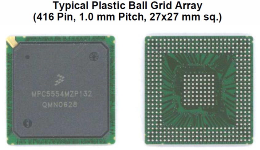
Figure 1. Typical PBGA Package (source: NXP Freescale) with area array solder balls on the laminate backside.
The first aspect to notice is that there are no leads around the periphery used to connect with the printed circuit board. In Figure 1, the image on the left shows the top side of a typical PBGA. The PBGA substrate is green in Figure 1. The term “plastic” in PBGA originates from the use of a polymer-based substrate. Semiconductor packaging substrates or laminates are typically epoxy-based with the most common thermosetting material being the Mitsubishi Gas Chemical (MGC) bismaleimide triazine (BT) resin. The BT resin is a combination of epoxy, cyanate ester, and bismaleimide and will be covered in detail in a subsequent post. It is interesting to note that the BT resin is not green. The soldermask used to define that solder pads and protect the outer surface of the PBGA substrate is green in color. The black material in the image on the left is the epoxy overmold. The right image in Figure 1 shows the back side of the PBGA.
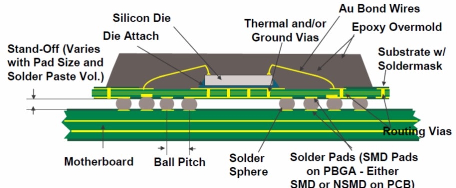
Figure 2. Schematic Cross Section of a Typical PBGA Package (source: NXP Freescale)
There is a lot to unpack in Figure 2. Compared with previous leadframe designs, there are several common elements, namely the use of a die attach adhesive, epoxy mold compound, and the electrical connection is made using gold wire bonds. The major difference is the use of a “plastic” laminate substrate instead of the metal leadframe. The semiconductor substrate is a multilayer printed circuit board with metal circuit traces and through holes (routing vias) to connect the front of the laminate with the ball pads on the back side. On the top surface of the substrate, there are metal pads where the gold wires are bonded. The pads on the semiconductor chip are arranged around the perimeter allowing for ease in wire bonding from the chip to the pads on the substrate. Additionally, there could also be a metal die pad to help with thermal management. In Figure 2, under the semiconductor die, there is a large metal pad where the die is placed. Under the die are copper plated thermal vias that aid in heat transfer from the die back to the back of the substrate.
Another big difference is the electrical connections to the printed circuit board are made using solder balls and a reflow process. In Figure 2, solder spheres (or balls) connect the semiconductor substrate with the motherboard. The PBGA manufacturers place the solder balls on the bottom surface of the substrate and ship to the customer. PBGA’s come with a standard ball pitch so that customers can mount them on the printed circuit board used in their device. PBGA’s ship with several types of solder sphere compositions [1].
Lead containing solder spheres:
- The most common is 62Sn36Pb2Ag (62% tin/36% lead/2% silver)
- Some may contain 62Sm37Pb
The drive to eliminate lead-containing materials has led to the use of lead-free solder sphere:
- The most common is 95.5Sn4.0Ag0.5 Cu (95.5 % tin/4% silver/0.5% copper), called SAC405
- Mobile devices may use SAC105 (98.5Sn1.0Ag0.5Cu)
- Some spheres may have the composition of 96.5Sn3.6Ag
The customer uses a pick and place process to position the PBGA on the printed circuit board and then subjects the entire package (PBGA and the PCB) to a high temperature reflow process that melts the solder, reflows and wets both pads, and upon cooling forms a metallurgical bond connecting the chip on the top side of the PGBA with the motherboard.
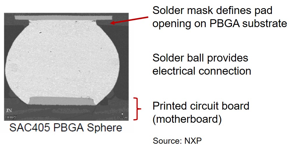
Figure 3. Cross-section of the SAC405 PBGA solder sphere after reflow [1]
In Figure 3 the solder sphere connects the pad on the BT semiconductor substrate to a pad on the motherboard. Note that a soldermask is used to define the area on the top pad that will be exposed to solder. Soldermasks are typically photo-imageable polymers (mainly epoxies) that can be patterned using UV light. Soldermasks are thermoset polymers that react upon UV exposure allowing openings in the soldermasks to be formed. UV curing and soldermasks will be covered in future posts.
This is really a great and informative one post about Plastic Ball Grid Array (PBGA) packages. Since last few years, the plastic ball grid array (PBGA) technology has been gaining industry-wide interest and commitment as the potentially lowest-cost package for high-I/O devices and even for some lower-pin count applications.
Hi, i know this is an old post but i would like to have an help. I’m a passionate repairer, i’m interested in reballing / reflowing precesses, i would like to know which is the material that covers the pads under the substrate… is it Silver? it’s important for understanding processes.. thanks!