
 In the last post, the processing of epoxy mold compounds (EMC) for standard leadframe packages, such as the Quad Flat Pack No Lead (QFN) shown on the left and PBGA packages was discussed. Leadframe, PBGA and flip chip packages continue to be high volume products and as such mold compound technology has matured. In the drive to have thinner electronic packaging, driven mainly by smartphone growth, new advanced packaging concepts have been developed.
Fan-out Wafer Level packaging is emerging as a high growth package type. The appeal of fan-out WLP is the elimination of the semiconductor substrate resulting in a thinner package. The fan-out WLP uses a completely different process to provide wiring and connections from the die (semiconductor chip) to the circuit board.
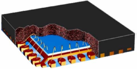
The portion of the Fan-out wafer level packaging (FOWLP) we will focus on in this post is the critical use of the EMC as the base for the redistribution layer (RDL). The unique aspect of the FOWLP package is the use of a reconstituted wafer. The traditional wafer is probed and the known good die are identified and sorted. The reconstitution process is shown in Figure 1.
Figure 1. Wafer reconstitution process for chip first, face down FOWLP (source: Nanium)
The reconstitution process starts with the preparation of the carrier wafer. It should be noted that the carrier wafer is circular and the entire FOWLP process utilizes existing wafer processing tools. A temporary bonding adhesive (red in Figure 1) is attached to the stainless steel carrier wafer (Step 1). In the next step, a pick and place tool is used to place the known good dies face down on the temporary bonding adhesive. Note: in the chip first approach (Figure 1), the die can be placed in the face down or in the face up orientation. For the mold compound discussions, we will use the face down (the original Infineon eWLB process flow). In step 3 in Figure 1, the carrier and dies are overmolded with EMC using a compression molding process. In step 4, the encapsulated dies are released from the carrier yielding the reconstituted wafer.
The emergence of FOWLP required the development of a new encapsulation process and subsequently required a new type of epoxy mold compound. The mold compound must have very low coefficient of thermal expansion (CTE) as close to the semiconductor chip as possible. In order to achieve a low CTE, the filler content was increased. Previous posts have discussed strategies used to increase filler loadings. The mold compound also must have good flow and be able to easily encapsulate the chips on the carrier.
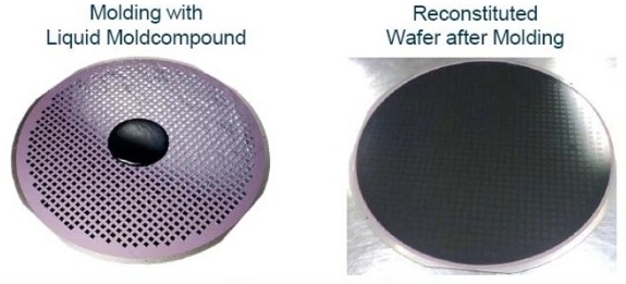
Figure 2. Molding with liquid molding compound (source: Nanium)
In Figure 2, an example is given for a liquid EMC. The individual known good dies are visible in the left image along with the initial dispensed liquid. After compression molding, all of the dies are encapsulated. The molding process uses three types of specialized epoxy mold compounds:
Liquid
- Nagase
- Pansonic
Solid Granules/Powder
- Hitachi
- Sumitomo
Film – Hitachi Chemical (Embedded Insulation Sheet (EBIS)
The Hitachi Chemical film is shown in Figure 3.
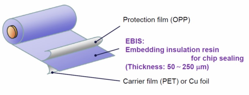
Figure 3. Hitachi Chemical Embedded Insulation Sheet (EBIS)
The interesting part of this approach is that the material is provided in roll form and potentially simplifies handling during the lamination/encapsulation process. From the Hitachi literature, the EBIS comes in thicknesses from 50-250 microns to allow for different resin contents and flow properties. The resin formulation is likely modified to have some flexibility at room temperature to allow for winding on rolls. The EBIS is used in the molding process in the same way as the liquid or solid forms. Figure 4 shows the wafer reconstitution process using the EBIS mold compound.
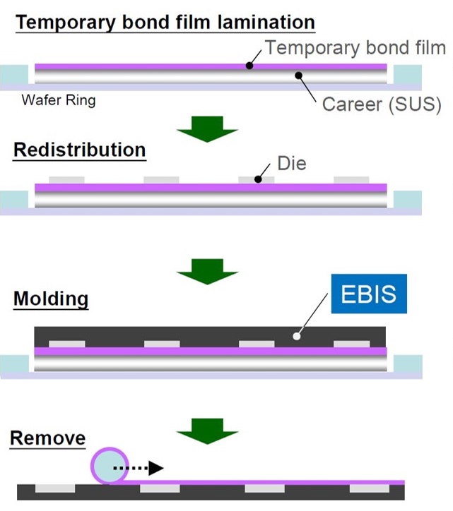
Figure 4. Wafer reconstitution process using the Hitachi Chemical EBIS mold compound.
In the next post, the compression molding process for liquid and solid epoxy mold compounds will be discussed.
Leave a Reply