
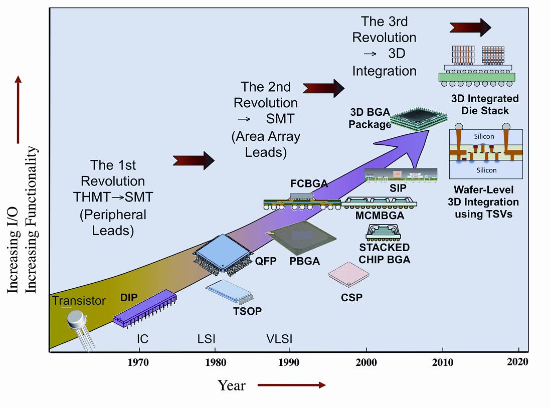
 The last several posts discussed the semiconductor packaging technology progression from dual-in-line (DIP) using through hole mounting, to quad flat pack packages that were surface mounted, to area array plastic ball grid array (PBGA) that were also surface mounted. As shown in the figure on the right, the first revolution was from through holes to surface mount. The second revolution was from peripheral array surface mount to area array packages such as plastic ball grid array (PBGA) to achieve higher I/O density. Another package in the second revolution is the flip chip ball grid array (FCBGA). Image from reference [1].
In the FCBGA package, instead of the chip leads being wire bonded from the periphery of the chip, solder balls are attached to the active side of the semiconductor chip and then the chip is mounted to a PBGA substrate using a reflow process to make the metallurgical connections. In Figure 1, the upper image shows a standard wire bond PBGA. Polymers are used in the die attach adhesives, the mold compound, and the rigid laminate substrate. The substrate is used to connect the chip leads to the printed circuit board via the solder balls on the bottom of the substrate.
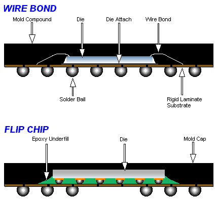
Figure 1. Comparison of a wire bond PBGA and a flip chip ball grid array (FCBGA) packages (courtesy of Amkor).
The lower image in Figure 1 depicts a flip chip ball grid array (FCBGA). The chip is attached to the laminate substrate suing solder balls and notice that the chip is oriented with the active side down, i.e. flipped over, thus the term flip chip. The rigid laminate substrate is similar to the wire bonded substrate, but has higher number of routing lines and potentially more through holes (and vias) to connect the circuit traces from the top side to the solder balls on the bottom.
Figure 2 shows the key elements in the FCBGA package.
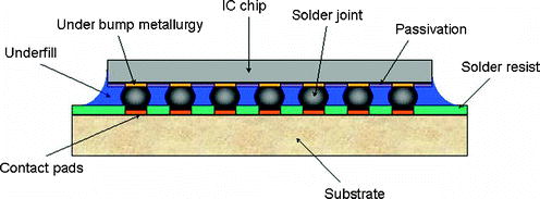
Figure 2. Cross-section of a typical flip chip BGA package
In the FCBGA, there is no die attach adhesive, but now an underfill is used as shown in Figure 2 as the blue material under the IC chip and between the solder balls. The purpose of the underfill is to stabilize the solder joints during thermal cycling. The coefficient of thermal expansion (CTE) of the IC chip is approximately 4 ppm/°C and the CTE of the glass cloth filled epoxy bismaleimide triazine laminate is approximately 17-20 ppm/°C. During thermal cycling, the CTE mis-match causes stress in the solder bumps. The highly filled epoxy underfill is used to help reduce the solder fatigue.
There are a couple of important things to point out in Figure 2. The process to make a FCBGA starts with placing the solder balls on the IC chip. This process is called bumping and the solder balls are placed on the IC chip pads (noted as under bump metallurgy in Figure 2). Various types and layers of metals are used in making the pad and we will not go into the details here. The solder balls make a metallurgical bond during a high temperature reflow process (used to melt the solder ball and join the solder ball to the IC chip pad). Once the solder bumps are attached, the bumped IC chip is attached to the laminate substrate using the flip chip attach process. Here, the IC chip is oriented face-down so the bumps will line up with pads on the laminate substrate. The solder bumps on the IC chip are connected to the pads on the laminate substrate using a second reflow process. During reflow, the solder balls melt and form a metallurgical bond between the solder ball and the pad on the substrate.
After the reflow process, the underfill is applied. The most common type of underfill is called capillary underfill. In the capillary underfill process, the underfill material is needle dispensed around one or two sides of the flip chip. Capillary force and surface tension pull the underfill under the die. The rheological profile and wetting characteristics of the underfill are very important and will be covered in a subsequent post.
Figure 3 shows the routing path from the die through the substrate to the printed circuit board.

Figure 3. Schematic of the routing path for a FCBGA
In Figure 3, the electrical path in the FCBGA is shown by the red lines. The IC chip (die) is connected to the package substrate pads via the solder balls (RDL or redistribution layer bump). There are circuit lines that connect the pads with the solder ball connection to copper plated vias (either mechanically drilled as shown in Figure 3, or laser drilled and subsequently copper plated). The electrical path then goes down through the via to the backside of the substrate. Again, there is a circuit trace that connects the via to a solder pad on the backside of the laminate (denoted by the red line on the bottom of the package substrate in Figure 3). During second level assembly, the FCBGA package is soldered to the printed circuit board (PCB) using a third reflow process. The FCBGA electrical signal then travels into the PCB through the solder bump and is routed on the surface of the PCB (red line on top of the green PCB).
References
Leave a Reply