Underfills are used to stabilize solder bumps and more recently copper pillar interconnections. The coefficient of thermal expansion (CTE) mismatch between the silicon chip and the polymer-based semiconductor substrate causes fatigue in the interconnections as the package thermally cycles.
Capillary underfills have been used for many years. In the case of capillary underfill, a highly engineered polymer formulation is dispensed around the edge of the flip chip and subsequently flows under the chip and in between the solder bump (or copper pillar) interconnects by capillary forces. Underfills are formulated to wet both the soldermask on the substrate and the die passivation layer on the chip to facilitate flow under the die.
The key underfill material requirements are:
- Optimize for stress control (warpage) by tailoring the glass transition temperature (Tg) and modulus
- High modulus (around 10 GPa)
- Mid-range Tg of approximately 90°C
- Low CTE (target < 25 ppm/°C)
- Low cure temperature (stress control)
- Low cure shrinkage (stress control)
- Tailored rheology depending on application
- Flow speed
- Good wetting to chip and substrate
- Good adhesion to chip and substrate
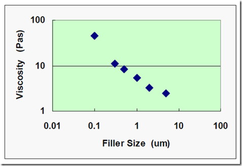
Flow (rheology) is a key challenge since the bump pitch is decreasing to 150 micron and less, the bump diameter is moving to < 50 micron, and getting to low CTE requires a high level of filler loading. As the filler loading increases, the viscosity increases significantly, slowing underfilling time. In the following figure, the viscosity is plotted as a function of filler size. Note the order of magnitude increase in the viscosity as the filler size approaches 0.1 microns.
Source: Namics at IMAPS 2013
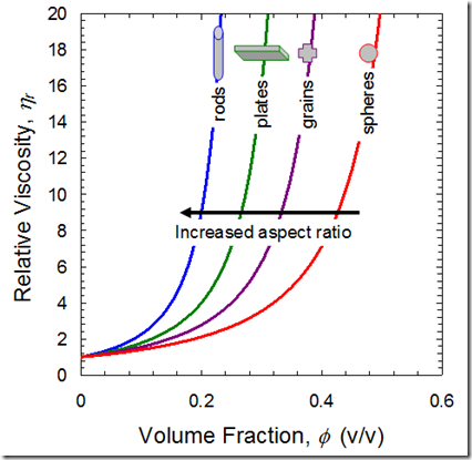
Not only does filler size impact the viscosity, but the filler loading and the filler geometry have a large influence on the viscosity. In the following figure the normalized viscosity is plotted as a function of filler volume fraction (loading) for various aspect ratios.
Current underfills use spherical silica fillers to allow maximum filler loading. As the aspect ratio of the fillers increase (grains, plates, then rods), the “viscosity penalty” occurs at progressively lower filler loadings. Thus, to get maximum filler loading and still have acceptable underfill times, careful selection of the right filler geometry is essential.
Additionally, the inner layer dielectric (ILD) in the chips is fragile and prone to cracking, necessitating careful management of stresses during assembly. The capillary underfill challenge has largely been met with a wide variety of underfill materials available from multiple suppliers. The current “best in class” underfills have CTE’s in the range of 25-30 ppm/oC using silica fillers with diameters of approximately 1 micron.
To get to lower CTE values, higher filler loading with smaller particle size is required. To achieve the < 25 ppm/oC value, fillers in the range of 0.3 microns will be used. With the advent of 2.5D and 3D integration, the thermal conductivity will need to be increased. Polymers are very good thermal insulators, so to increase the thermal conductivity, fillers such as boron nitride with much higher thermal conductivity will be needed.
In the next post we will discuss the new approaches to underfill 2.5D and 3D packages.


Leave a Reply