This post will outline the next blog series on polymer challenges in electronic packaging. Polymers are key enablers of electronic packaging. For those new to electronics, the term “packaging” is used for the technology utilized to connect a semiconductor chip (or die) to various types of substrates and eventually to a multilayer printed circuit board (PCB). Electronic packaging is required to take the very fine pitch (or interconnect spacing) on the chip and “fan-out” or re-distribute to a much wider spacing or pitch on the PCB. The subsequent series of posts will focus on the polymer aspects assuming the reader has at least a basic understanding of electronic packaging. There are many good texts and other resources available if you need an electronic materials packaging primer.
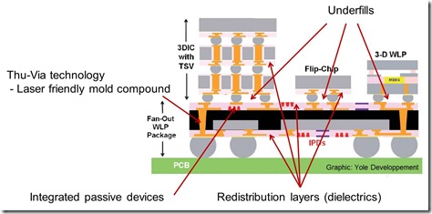
In the following figure (Courtesy of Yole Developpement), one can observe there are some key polymer applications that will enable the next generation of 2.5D and 3D packaging.
Some of the key polymer challenges are:
- Underfills; low CTE and thermally enhanced pre-applied and wafer level underfills
- Wafer level packaging; CTE mismatch compensation for large die and fan-out die
- Enhanced mold compounds with laser drillability
- Improved dielectrics for redistribution layers
- Small die/ high power density; Thermal dissipation becomes an issue
- Cost-Performance
- Require very high yield process
- Innovation in materials and process simultaneously
In the coming posts, we will dive into more detail on each of the key polymer challenges with a focus on the polymer and formulation developments required for successful 2.5D and 3D integration.


Leave a Reply