 In the last few posts in this series, we have been discussing polymer challenges in embedded wafer level packaging (eWLP). The last topic to discuss is the redistribution layers and a few comments about manufacturing to achieve very high yield processes.
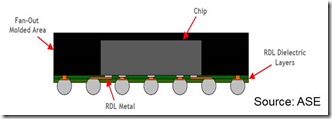
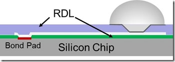
First let’s talk about the polymer redistribution layers used in fan-out eWLP. The key aspect of the fan out package is the concept of using redistribution layers to route out the I/O’s from the chip to the semiconductor package substrate. In the following figure, the redistribution layers are shown schematically:
If you recall from the process flow, after the mold compound encapsulation process, the front face of the die is not covered allowing subsequent deposition of the polymer redistribution layers. Typical polymers used for the redistribution layers are photo sensitive polyimides (PI or PSPI), polybenzoxazole (PBO) and benzocyclobutene (BCB). In 2011, polyimide accounted for about 50% of the polymers used in WLP, with BCB (Dow Chemical Cyclotene) at 22% and PBO at 17% (Yole Devellopement). HD Micro Systems (Hitachi/DuPont) supplies the majority of the polyimide and also sells PBO. Toray and Asahi Kasei also provide polyimides to the packaging market.
An interesting distinction between a photoresist and the photo-sensitive polymer dielectrics used in eWLP is that the redistribution layers are a permanent part of the package structure. Unlike a photoresist that gets removed after imaging, the photo-sensitive dielectric layers must be formulated to have good mechanical and electrical properties.
Permanent dielectric material requirements:
- Improved toughness; bond pads on top of polymer will add stress that the polymer must accommodate
- Decrease the cure temperatures; lower temperature processing will help to decrease warpage
- Faster cure times to increase the process throughput (UPH)
- Lower CTE to address the CTE mismatch between the die and the packaging polymers
- Improved resolution for photo-sensitive dielectrics; decreasing bump size and increased bump density
Most unfilled polymers have an inherently high CTE in the range of 50-80 ppm/C below Tg. Typically fillers are used to lower the CTE since the inorganic fillers have significantly lower CTE’s.
Strategies to lower CTE:
- Silica fillers with multimodal distributions (generational packing)
- Thermally conductive filler like boron nitride yield double benefit
- High filler loading significantly increase the viscosity
- High filler loadings adverse affect the light transmission during UV exposure of photo-sensitive polymers
- Molecular orientation of the polymer chains
The last strategy is what I call “molecular engineering” since polyimide films like Upilex from UBE have well ordered molecular packing in the plane of the film. This results in a low in-plane CTE from the molecular orientation. The out-of-plane CTE is typically higher, but since these are used as thin films, this is not usually a problem.
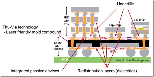
The last issue to address in the eWLP development is the manufacturing process impacts. In the following figure (Yole Devellopement) shows a schematic of how complex 2.5D and 3D packaging will become.
For cost control, the OSAT’s must have very highly yielding processes. Additionally, interfaces are the enemy!
- Adhesion issues
- Migration path leading to reliability issues
- CTE mismatch and resulting stresses on the interfaces
- Multiple process steps
- Material and process development must occur concurrently, since the process/material interactions can be significant.
Remember the concept of Rolled Throughput Yield (RTY) is that the final yield is the product of all of the successive process step yields. For example if you have a five step process and each is yielding at 99%, the RTY would be:
0.99 x 0.99 x 0.99 x 0.99 x 0.99 = 0.95 (or 95% yield)
In most very high volume manufacturing processes, this level of RTY would not be acceptable.
eWLP Polymer Summary
- Significant progress in developing advanced polymer materials for 2.5D and 3D
- eWLP challenges being addressed for
- mold compound
- redistribution layers
- optimizing manufacturing processes
- Achieving high reliability and cost control requires and unending focus on yield (process-materials-interfaces)


Leave a Reply