Polymer Innovation Blog

Practical tips and advice for polymer, innovation and product development professionals

Polymer Innovation
  • Home
  • eBooks
    • Polymers in Electronic Packaging
    • Rheology of Thermosets eBook
    • Practical Tips for Curing Thermosets
    • Thermoset Characterization
    • Dielectric Cure Monitoring of Thermosets
    • Introduction to Biopolymers and Bioplastics
  • Videos
    • Core Curriculum: 3 Part Video Series
    • Characterization of Thermosets: 4 Part Video Series
    • Advanced Thermoset Cure Kinetics: 3 Part Video Series
    • DSC of Polymers: 5 Part Video Series
    • Thermoplastics: 5 Part Video Series
  • Services
    • Consulting
    • Polymer Expert Witness
  • Learning Center
    • White Paper
  • Why Jeff?
    • Speaker Info
  • Contact
  • Subscribe
  • Members
    • Login
    • Logout

Polymer Challenges in Electronic Packaging: Part 7 Embedded Wafer Level Packaging Process Flow

November 25, 2013 By Jeffrey Gotro 1 Comment

In the last post in this series we introduced the embedded wafer level package concept.  In this post we will dive in a little deeper and look at the process and some of the polymer challenges.

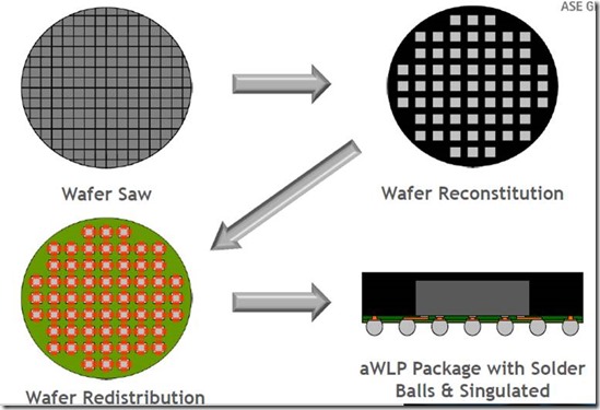
A high level overview may be seen in the next figure (source: ASE Group)

embedded wafer level process flow at a high level

The finished wafer is singlulated using traditional dicing methods to yield individual chips that are mounted on a substrate to form a “reconstituted” wafer.  The density of the chips on the reconstituted wafer is governed by the size of the fanout required by the redistribution layer.  The chips are mounted face-down on the carrier with care to ensure precise and repeatable placement.  The wafer and chip array is over molded using a specially developed mold compound.  We will discuss some of the key mold compound material parameters later.  In the upper right corner, the reconstituted wafer is seen after molding.  Notice that significantly less chips are mounted on the reconstituted wafer.  After molding the back side of the reconstituted wafer is polished to ensure a planar surface.  An addition thin layer of epoxy mold compound is then applied to the backside to eventually protect the top of the eWLP package.  The next major step is to apply a polymer redistribution layer on the top side (exposed bumps from the chips are now accessible).  Typically several layers of redistribution layers are applied and photoimaged.  In the lower left corner of the figure above, the redistribution layers have been imaged and plated.  The next step is to apply the desired interconnection method (either solder bump or plate copper pillar’s) onto each chip.  The final step is to singulate the individual packages from the reconstituted wafer.

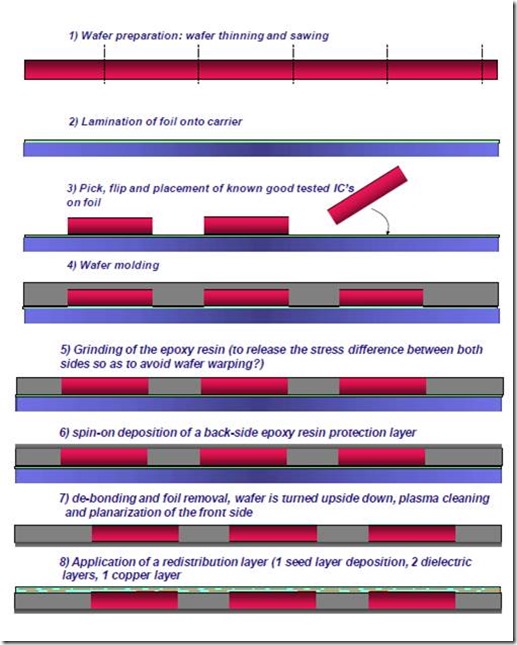
The detailed process flow (Source: Infineon) is given in the following figures:

Infineon detailed eWLP process flow1

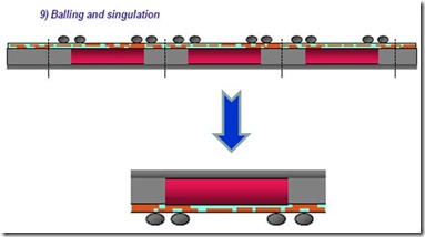
The final interconnect attach (in this case solder ball bumping) and singulation is performed to yield the final package:

Infineon eWLP process flow2

Polymer Challenges

Mold Compound optimization is a key enabler for embedded wafer level packaging.  The molding process requires a mold compound with low viscosity and a thixotropic (shear thinning) index near 1 which means at the molding temperature the highly filled liquid is Newtonian (no shear rate dependence).  In order to control the warpage and die shift, the filler content needed to be increased to 92 to 95% which impacts the viscosity and flow.  To achieve these high loading levels, multi-modal silica particle size distributions were used.  In addition, the resin-particle interactions play a role in the viscosity so care must be taken to optimize the surface of the fillers.  This is critical as the filler size decreases, resulting in a large increase in the surface area and thus more particle-particle interactions.  In many cases, the fully cured mold compound needs to be laser drillable to enable package stacking.

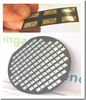
eWLP mold compound

In the picture on the left, the top image shows a portion of the embedded die surrounded by mold compound.  The image on the bottom is a reconstituted wafer after molding.

Key material properties are:

  • Low CTE to match silicon
  • Controlled shrinkage
  • Low stress after molding


Source: NXP

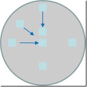
Since the step after molding involves depositing and imaging the redistribution layers, the cure shrinkage needs to be uniform.  During curing, the dies will shift toward the center of the wafer, the farther toward the edge the larger the shift.  In the figure below, if the shrinkage is not uniform, then the amount of movement will not be consistent across the wafer making registration of the redistribution layer photomask and the imaging process a challenge.   Careful formulation of both the resins (optimized for low cure shrinkage) and surface treated fillers for CTE control is necessary for high yield processing.

die shrinkage during eWLP processing

One can see that polymers play a critical role in the packaging and reliability of 2.5D electronic packages used in many applications such as smartphone, computer, and other complex electronic devices.
Share on LinkedIn Share

Filed Under: Uncategorized

« Second Generation Biomass Feedstock 5: The Complex Pretreatment Landscape
Happy Thanksgiving! »

Leave a Reply

Your email address will not be published. Required fields are marked *

Polymer Innovation Blog

I’m Dr. Jeff Gotro and welcome to the Polymer Innovation Blog. Over the last 40 years I have been involved in polymer research, along with product and process development. I acquired invaluable experience working for IBM, AlliedSignal, Honeywell, Ablestik Labs (now Henkel) and in multiple consulting projects. In this blog, I (along with some guest contributors) will share our experiences, tips, and “tricks of the trade” to get more out of your innovation efforts and discuss new trends and technical advances in the polymer industry.
View Jeff Gotro, Ph.D., CMC's profile on LinkedIn

Innocentrix, LLC


Click to Visit Website

plastics expert witness
Click for More Information

Subscribe by Email

Search the Blog

Polymer Video Training

Visit our Video Store

Polymers in Electronic Packaging

polymers in electronic packaging Are you confused about what is electronic packaging? Have you ever wondered what type of polymers and polymer-based composites are used in electronics? Learn More...

Practical Tips for Curing Thermosets

practical tips for curing thermosets Have you ever had a question about the degree of cure or is your part fully cured after processing? Confused about what is gelation or how does vitrification impact thermoset curing? Learn More...

Rheology of Thermosets

rheology of thermosets Have you ever had a question about measuring the rheological properties of thermosets Didn’t know what is the right experimental approach to get the right rheological information? Learn More...

Dielectric Cure Monitoring of Thermosets

Dielectric Cure Monitoring of Thermosets Do you have a need for an in-situ cure monitor for a thermoset process but don’t know where to start? Are you confused about the terminology used in dielectric spectroscopy? Learn More...

Introduction to Biopolymers and Bioplastics

Introduction to Biopolymers and Bioplastics Would you like to know how sustainable are bio-based polymers? Or what is the market size and growth rate for bioplastics? Or have questions about the biomass supply chain? Learn More...

Thermoset Characterization

Thermoset Characterization Have you ever had a question about how to measure a physical property of a thermoset? Confused about what is gelation or how does vitrification impact thermoset curing profiles? Or wondered how to measure the glass transition temperature of an epoxy or polyester composite? Learn More...

Amazon.com Bookshelf

Robert's Rules of Innovation Thermal Analysis of Polymers Order

Copyright © 2025 Innocentrix, LLC · All Rights Reserved