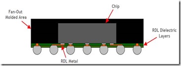
In this post we will discuss a new packaging type generically called embedded wafer level packaging. Many OSAT’s have different names, but the concept is pretty much the same.
Source: ASE
In traditional semiconductor packaging, wafers are typically bumped and singulated prior to packaging and in most cases the die is attached to the package. The most common packages are leadframe packages where the die is attached using a die attach adhesive and the electrical interconnects are made using wire bonding. As the density increased, the plastic ball grid array was introduced where again a single die was attached to a polymer-based laminate with an area array of solder balls on the back side (hence the term plastic ball grid array or PBGA).
With the increasing demands of mobile computing, smaller footprints, higher I/O chips, a single bumped die was placed on the PBGA substrate, but using flip chip technology. In the case of flip chip packaging, the bumped chip is pick-and-placed onto the PBGA substrate and subsequently solder reflowed to make electrical connections thru the solder bumps. After reflow, the flip chip bumps are encapsulated (the area between the bumps and the chip and PBGA) using a capillary underfill to protect the solder bumps from fatigue during temperature cycling.
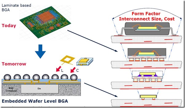
The packaging evolution is shown in the following figure:
On the right side one can observe the progression from a leadframe, to PBGA (with wirebonds), to a flip chip PBGA (with underfill in purple), to the next generation called embedded wafer level BGA. As we will see, the packaging is now applied at the wafer level enabling multiple die to be packaged on a single wafer. The package shown above is called a wafer level fanout since the interconnections from the die fan out to a larger pitch using redistribution layers applied to the top surface of the chip/package.
New polymer materials were developed for:
- Mold compound used to encapsulate the die required very high filler content
- Molding required a very low viscosity despite the 90-95% by weight silica filler loading
- Laser drillable mold compounds
- Controlled shrinkage and warpage control
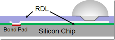
- Redistribution layers (RDL) using photosensitive polymers with improved imaging resolution
- Improved RDL toughness
- Decreased cure temperatures and lower CTE for the RDL to reduce stress
In the next post the manufacturing process for eWLP will be presented.


Excellent source of compiled information. Thanks!