
![]() In our series on polymers in electronics late last year, materials for fan-out wafer level packaging were covered in some detail. I attended the Electronic Components and Technology Conference (ECTC) the last week in May and in the next several posts, I will highlight what I see as some of the emerging themes. With fan-out wafer level packaging (or whatever name the various suppliers use) in high volume manufacturing, one of the new themes that got a lot of attention was heterogeneous integration. On Tuesday, May 28, there was a day long Heterogeneous Integration Roadmap Workshop. Unfortunately, I was unable to attend since I was teaching my professional development course on Tuesday.
In our series on polymers in electronics late last year, materials for fan-out wafer level packaging were covered in some detail. I attended the Electronic Components and Technology Conference (ECTC) the last week in May and in the next several posts, I will highlight what I see as some of the emerging themes. With fan-out wafer level packaging (or whatever name the various suppliers use) in high volume manufacturing, one of the new themes that got a lot of attention was heterogeneous integration. On Tuesday, May 28, there was a day long Heterogeneous Integration Roadmap Workshop. Unfortunately, I was unable to attend since I was teaching my professional development course on Tuesday.
From a polymeric materials perspective, the following areas were discussed in multiple papers:
- Packaging approaches to heterogeneous integration (wafer versus panel)
- Fan-out Panel Level Packaging (FOPLP)
- Film-based epoxy mold compounds (EMC)
- Improvements in polymer redistribution layers (RDL)
One of the benefits of the various embodiments of the fan-out packaging approaches is the ability to package multiple types of dies in a single fan-out package, thus the term heterogeneous integration. Multiple packaging suppliers and industry consortia are working on this approach. Cost reduction is always a key driver in packaging. One approach to lower the fan-out packaging cost is to build the packages on a panel rather than a round wafer. Figure 1 shows the panel roadmap based on Yole Developpement’s work.
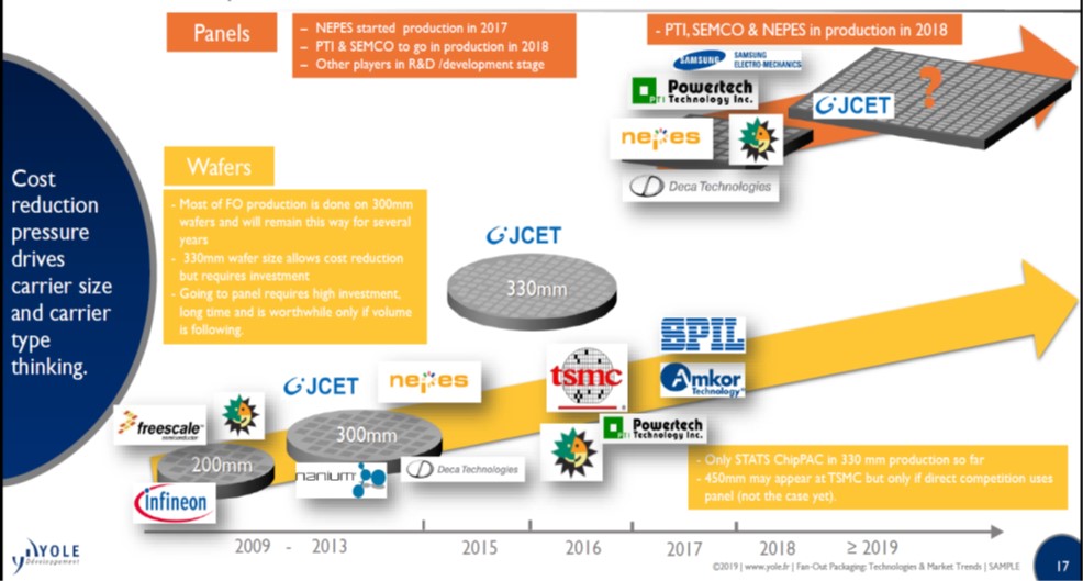
Figure 1. Fan-out packaging roadmap in terms of substrate (wafer versus panel)
The round format was originally adopted since many of the required tools were available to process in the round 300 mm format. Figure 1 shows the main manufacturing companies that are currently supplying FOWLP. There are many of the largest semiconductor packagers (ASE, Amkor, and JCET) along with multiple technology providers such as Nanium (now part of Amkor), Deca Technologies (working with ASE) and Powertech.
In the upper right corner in Figure 1, the companies that are pursuing panel level fan-out are presented. Note that ASE/Deca, JCET, Powertech, Samsung and Nepes are reported to be active in panel development. At the ECTC exhibit, Deca had a 600 X 600 mm panel on display in their booth.
Figure 2 shows a timeline for manufacturing readiness for fan-out panel level packaging.
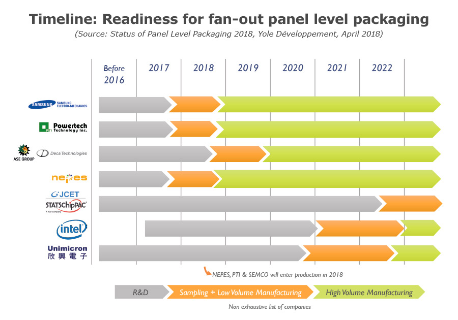
Figure 2. Manufacturing readiness for fan-out panel level packaging (source: Yole Developpement)
It is interesting to note that some of the companies in panel level packaging have deep expertise in fabricating semiconductor substrates such as ASE, Samsung and Unimicron. Note in Figure 2, Deca Technologies are ASE are listed on the same line reflecting the technology partnership between the two companies. It is interesting that Unimicron is part of a large consortia that is exploring panel level fan-out using a more conventional circuit board type process. John Lau presented at paper at ECTC on the panel approach to heterogeneous integration [1]. Figure 3 shows the cross-section of the panel used to package four chips in the fan-out panel level package (FOPLP).
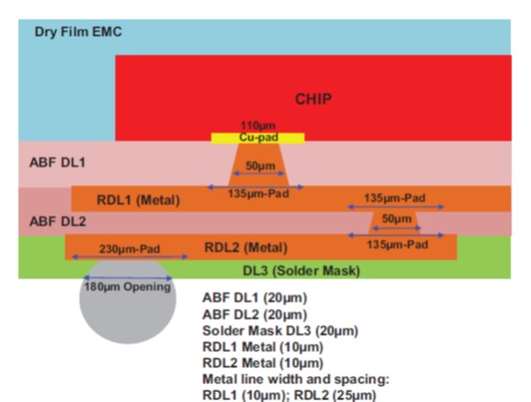
Figure 3. Cross-section from the Unimicron process from reference [1].
In Figure 3, there are several materials to note. The approach has been to use a printed circuit board process as much as possible, both to lower cost and leverage the PCB processes and expertise of the member companies. The first material to note is the use of Ajinomoto build-up films for dielectric layers one and two (ABF DL1 and ABF DL2). None of the FOWLP on round wafers used an Ajinomoto material for the RDL dielectric. In the High Density Interconnect (HDI) circuit board process, Ajinomoto build-up film has been extensively used for decades. In addition, the Unimicron process uses a dry film epoxy mold compound (EMC) as show in the light blue region in Figure 3.
The use of a dry film EMC makes sense in that the equipment size needed to compression mold either liquid or powder EMC would be costly and large. Printed circuit board processes are used to handling dry films for example dry film photoresists.
The next post will cover more details of the dry film EMC and the ABF redistribution layers.
Reference
- John Lau et. al. “Feasibility Study of Fan-Out Panel-Level Packaging for Heterogeneous Integrations, 2019 IEEE, 69th Electronic Components and Technology Conference. The authors were part of a consortium consisting of the following companies; Unimicron, ASM Pacific Technology Ltd, Dow Chemical Company, Jiangyin Changdian Advanced Packaign Col, Ltd., Indium Corporation, Huawei Technlogies Co. Ltd., Hong Kong University of Science and Technology.
Leave a Reply