
The last post discussed the future transition to a panel format for Fan-Out Wafer Level Packaging. The transition will occur over the next several years as the volumes ramp for wafer level packages. Yole’ Developpement has investigated the potential timing for the panel process. Figure 1 shows the timing of panel R&D, sampling and low-volume manufacturing (LVM) and high-volume manufacturing (HVM) out to 2023. The chart provides an interesting look into the manufacturing landscape. HVM is not available until at least 2019 for three packagers and Advanced Semiconductor Engineering (ASE) (the largest OSAT) has publicly disclosed HVM for panel in 2020 consistent with the projection in Figure 1.
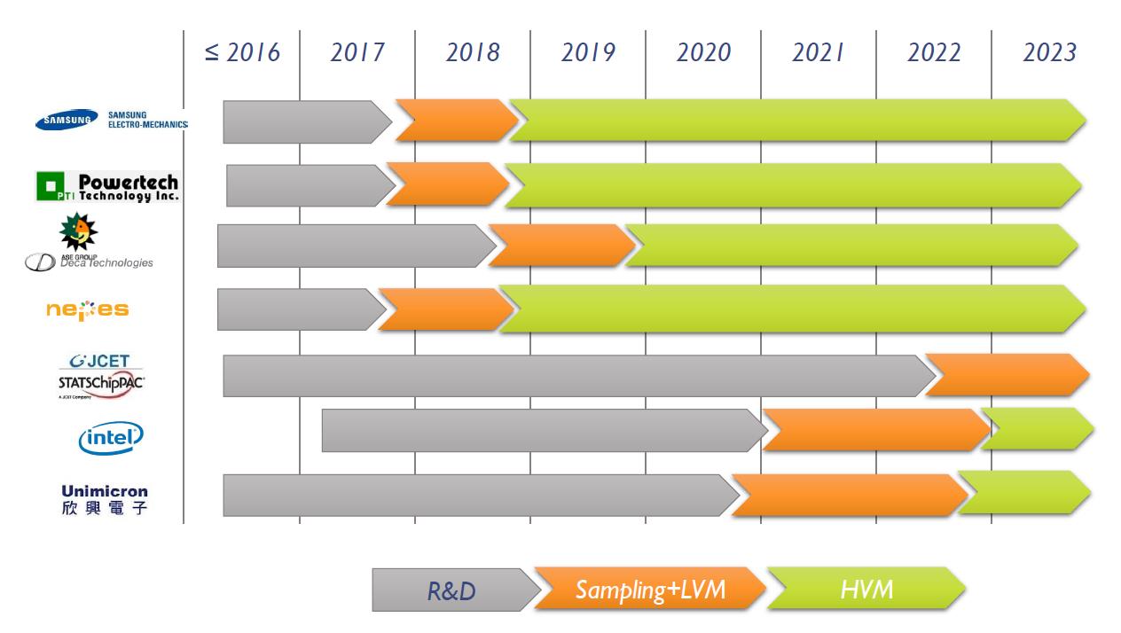
Figure 1. Manufacturing landscape for panel-level Fan-Out Wafer Level Packaging (source: Yole’ Developpement)
As discussed in the last post, the current Fan-Out Wafer Level Packaging format uses a 300 mm (and some 200 mm) round wafer. The existing equipment set was easily adapted for the round format with the exception of the epoxy molding process. Transitioning to a panel format will also require some significant new tooling development. Currently, there is no standard format for panels in FOWLP. In printed circuit board and semiconductor substrate manufacturing there are established panel sizes, typically 18” x 24” (approximately 450 mm x 600 mm).
Advanced Semiconductor Engineering (ASE) has partnered with DECA Technologies to use their Adaptive Patterning and Adaptive Routing technologies in the panel process. ASE has also settled on a 600 x 600 mm panel. The rationale is that the larger panel can be segmented into for 300 x 300 mm quadrants as shown in Figure 2.
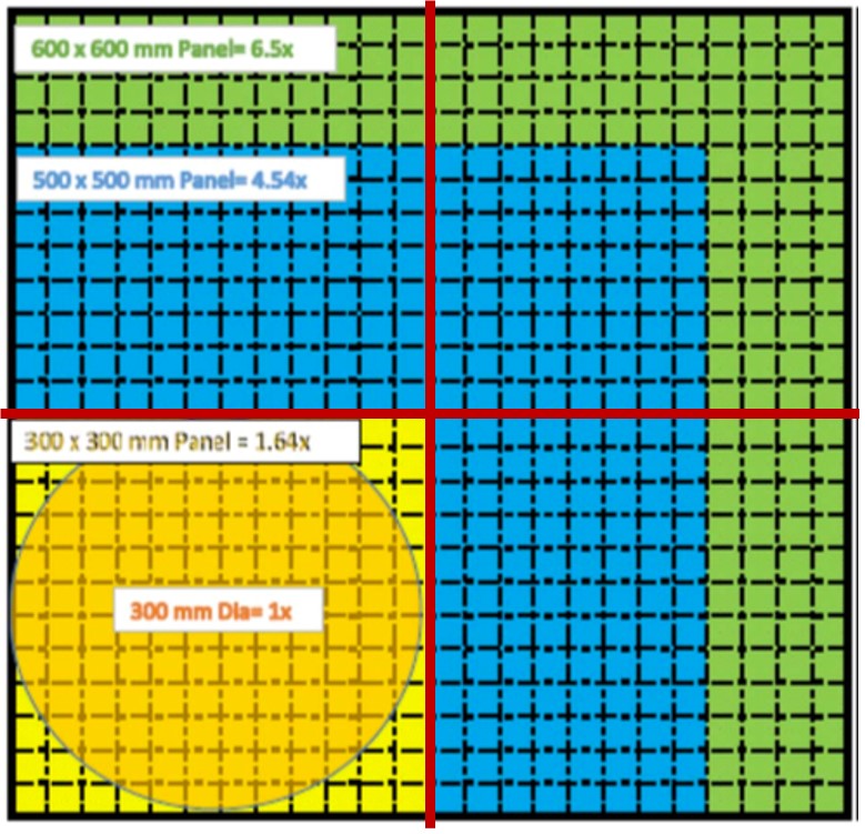
Figure 2. ASE panel approach using a 600 x 600 mm square panel.
Additionally, there are several advantages of the 600 x 600 format:
- The current 300 mm round re-constituted wafer tooling would be adaptable for processing one quadrant at a time (see the lower left quadrant in Figure 2).
- Processing one quadrant at a time (more specifically the photoimaging process) would allow for multiple designs to be made per panel (i.e. one design in one or more quadrants)
- Panel level processing will ultimately result in lower cost per unit
What will be some of the major technical challenges? At a high level, thin panel handling will need to be addressed, since currently the round re-constituted wafers are processed on a rigid carrier. Secondly, the epoxy molding compound (EMC) encapsulation process will need to be developed for a panel format. Liquid EMC will be difficult to process in the panel format. In response to the need for a panel level EMC, several EMC suppliers have developed EMC in sheet form. As shown in Figure 3, Hitachi Chemical has developed an embedded insulation resin for chip sealing called EBIS.
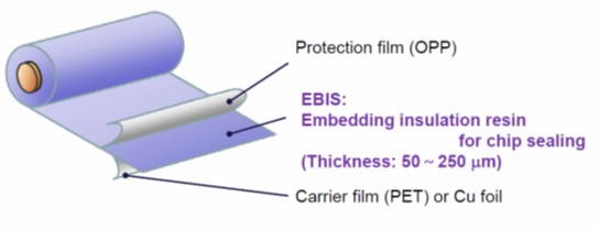
Figure 3. Film-based epoxy mold compound for FOWLP (source: Hitachi Chemical)
In this form, the highly-filled epoxy base resin is coated onto a carrier in thicknesses ranging from 50 – 250 µ). The EMC film is used in a vacuum lamination process to encapsulate the chips on the re-constituted wafer or panel. Ajinomoto Fine-Techno has also developed two types of epoxy mold compounds; liquid EMC (called the MI Series) for wafer level fan-out packages and a film EMC (called the LE Series) for the panel level fan-out process.
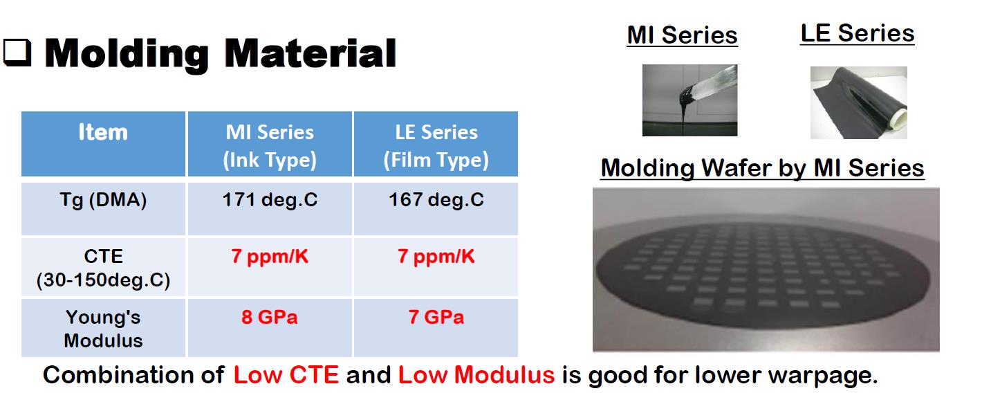
Figure 4. Two types of epoxy molding compounds for fan-out packaging (source: Ajinomoto Fine-Techno LTD)
From the table in Figure 4, the glass transition temperature (Tg) is in the range typical of cured EMC. One property to note is that for the FOWLP process, the coefficient of thermal expansion (CTE) needs to be very low and is usually matched to the CTE of the carrier. Note that the CTE reported in Figure 4, is identified as the CTE below the glass transition temperature. I also like the details provided which indicate the Tg was measured using dynamic mechanical analysis (DMA) and the CTE reported was over the temperature range of 30-150°C. The major driver for lowering the CTE and modulus is to reduce warpage after EMC processing.
There has not been a lot of discussion at the recent packaging meetings about the process that may be used for film EMC. ASE has extensive experience in the manufacturing of complex semiconductor substrates, so a good assumption would be that the EMC would be vacuum laminated onto the reconstituted panel. Precision vacuum lamination processes have been developed for laminating build-up films (Ajinomoto and Sekisui) onto high density interconnect (HDI) printed circuit boards.
The next post will cover more on the materials and processes required for panel level fan-out packages.
Leave a Reply