
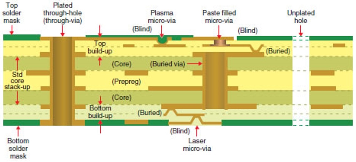
Figure 1. Cross section of FC-BGA multilayer semiconductor HDI substrate
The driving force for adoption of flip-chip packaging was the rapidly increasing bump count on logic chips thus requiring a higher routing density semiconductor substrate. The wire bond PBGA typically utilized a two sided BT substrate which provided adequate fan-out and communication with the backside bump grid. The bump pitch (spacing between the solder balls) was decreasing and the number of bumps (now copper pillars) was significantly increasing. Figure 1 shows a schematic of an 8 layer semiconductor substrate. The construction is termed a High Density Interconnect (HDI) substrate. A specific nomenclature has been adopted to describe HDI substrates. Notice in Figure 1, there are two layers of build-up film on each side and the core stack-up has 4 circuit layers. The nomenclature for this construction is a 2+4+2 (2 build-up + 4 core layers + 2 build-up layers).
The glass/BT epoxy core provides rigidity and locations for both buried vias and through vias. In Figure 1, the BT epoxy is labeled (core) and (prepreg). The BT epoxy core has 4 layers of circuitry and is noted on the left side of Figure 1 as the standard core stack-up. The BT epoxy core stack-up is fabricated first and then build-up layers are placed on the top and bottom.
The BT epoxy core substrate properties:
- Tg of 185°C (DSC) or 205°C (DMA)
- Woven glass cloth laminate with high reliability
- Highly resistant to conductive anodic filament (CAF) formation leading to very high reliability
- High peel strengths with standard copper
- Excellent thermal and moisture resistance
The primary substrate core supplier is Mitsubishi Gas Chemical (MGC) and has supplied the industry with bismaleimide triazine (BT) laminates since the early 1980’s.
In Figure 1, the nomenclature of (prepreg) is mis-leading. The two (core) layers are circuitized on both sides using standard printed circuit board techniques. The cores are electrically tested and yielded. The next step is to place prepreg between the two cores and use a second lamination process to soften and flow the prepreg and fully cure resulting in a four layer core. Prepreg is a partially cured BT epoxy resin impregnated into woven glass cloth. Prepreg is made by impregnating the woven glass fabric with the BT epoxy resin, drying the solvent and partially curing (termed B-staging). The important aspect of prepreg is that the conversion during the B-stage must be controlled to be lower than the gel point. After B-staging, the BT epoxy glass cloth is cooled to room temperature where it is an ungelled glass. During the subsequent lamination process, heat causes the prepreg to soften, flow, wet the circuit traces, bond the layers together, and fully cure. The core can subsequently be mechanically drilled forming the buried via on the right side in Figure 1.
Once the four layer core is fabricated, additional dielectric layers are applied to each side of the core.
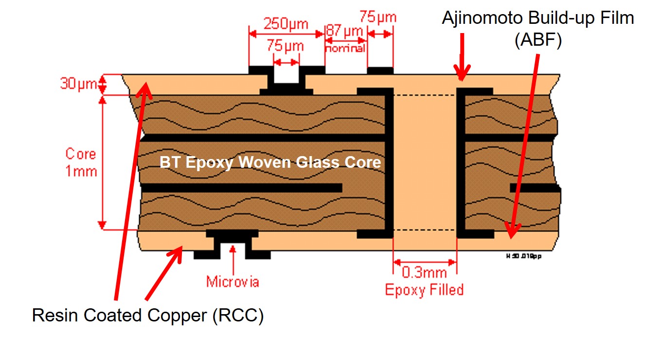
Figure 2. Schematic of a BT epoxy woven glass core with one layer of build-up film on each side.
Once the 4 layer core is completed (as shown in both Figures 1 and 2), additional thin dielectric layers are added to both sides of the core. The dielectric layers can be added as a build-up film (Ajinomoto Build-up Film or ABF) on the top side or Resin Coated Copper (RCC) on the bottom side. The dielectric films are capable of being laser drilled and do not contain woven glass fabric. In Figure 2, laser drilling form the microvia which allows connection from the core to the top surface. Various types of lasers are used to form the microvia and subsequent copper plating processes allow the electrical interconnection to the top and bottom of the HDI substrate. Figure 2 shows a 1+4+1 HDI substrate.
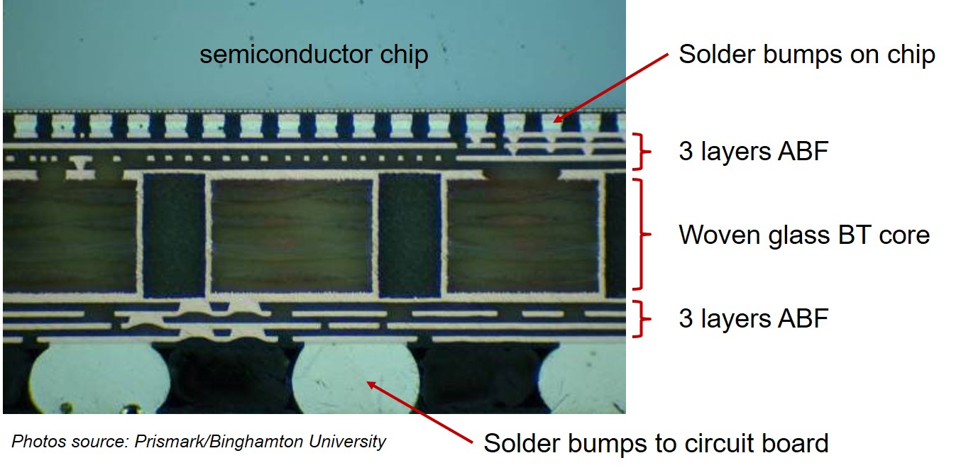
Figure 3. An example of a HDI substrate used for a Flip Chip BGA
Figure 3 is an example of a fairly complex HDI structure (3+4+3). Note in this cross-section the internal circuit layers are not visible in the core. The semiconductor chip is on the top and is solder ball connected to the top of the HDI substrate. There are 3 layers of ABF on the top and bottom. Note the close bump spacing on the semiconductor chip compared with the large and widely space solder balls on the bottom of the HDI substrate. The circuit lines are very small in the top ABF layers. The woven glass BT core provides rigidity and internal power planes. Note this structure has buried through holes (made using mechanical drilling). Looking at the shape of the microvias indicates these were laser drilled and copper plated.
The next post will discuss the materials and process used to apply the build-up films.
Leave a Reply