Polymer Innovation Blog

Practical tips and advice for polymer, innovation and product development professionals

Polymer Innovation
  • Home
  • eBooks
    • Polymers in Electronic Packaging
    • Rheology of Thermosets eBook
    • Practical Tips for Curing Thermosets
    • Thermoset Characterization
    • Dielectric Cure Monitoring of Thermosets
    • Introduction to Biopolymers and Bioplastics
  • Videos
    • Core Curriculum: 3 Part Video Series
    • Characterization of Thermosets: 4 Part Video Series
    • Advanced Thermoset Cure Kinetics: 3 Part Video Series
    • DSC of Polymers: 5 Part Video Series
    • Thermoplastics: 5 Part Video Series
  • Services
    • Consulting
    • Polymer Expert Witness
  • Learning Center
    • White Paper
  • Why Jeff?
    • Speaker Info
  • Contact
  • Subscribe
  • Members
    • Login
    • Logout

Polymers in Electronics Part Six: Redistribution Layers for Fan-Out Wafer Level Packaging

May 1, 2017 By Jeffrey Gotro 1 Comment

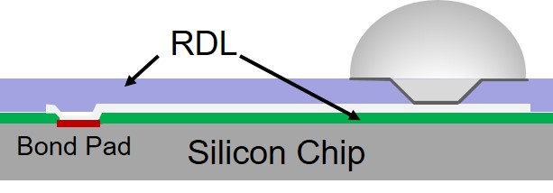
The last post introduced the use of a polymer dielectric as a redistribution layer (RDL) as a means to fan-out circuit traces from the chip to the backside of the package. In the image on the left, the RDL layers are shown in green (RDL1) and purple (RDL2).  The RDL layers (also called dielectric layers) are applied to the reconstituted wafer and imaged using photolighography.  This post will discuss more details of the RDL process for FOWLP.

Polymer Challenges for RDL’s

  • Lower cure temperatures
    • Target is 200°C (compatibility with epoxy mold compound)
  • Minimize warpage
    • Low film stress
    • Lower elastic modulus
  • Achieve high reliability
    • Low modulus
    • High elongation (ductility)
  • Chemical resistance
  • Good resolution during photolithography (lines/spaces and vias)
  • Ability to effectively planarize reconstituted wafer surface

Figure 1 demonstrates one of the challenges in the chip-first face-down approach to FOWLP.

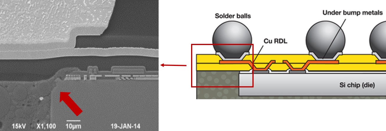
Figure 1. SEM image of the top surface of the chip after application of redistribution layers (SEM image from Nanium). 

After wafer reconstitution, at the corner of the chip where it meets the mold compound is not planar.  In Figure 1, the red arrow shows the thickness discontinuity at the corner of the chip.  The RDL must be capable to accommodate the slight difference in height during the application of the RDL material.  In Figure 1, the RDL is capable of doing a reasonable job planarizing the epoxy mold compound/chip surface.  The SEM image in Figure 1 shows both RDL’s and the solder ball attached to the plated via connecting RDL1 with RDL2.

The first dielectric materials for fan-out were photosensitive polyimides such as HD 4100 (HD Microsystems, a joint venture between Hitachi Chemical and DuPont).  HD 4100 is a negative tone photo-imageable dielectric.  The major drawback for polyimide systems is the very high cure temperatures in the range of 350-390°C which caused compatibility issues with the epoxy mold compounds.  Several material suppliers have developed lower temperature curing dielectrics.  HD Microsystem has introduced HD 8940 polybenzoxazole which cures at 200°C.

The process for application of the photosensitive dielectric materials (RDL1 and RDL2) is shown in Figure 2.

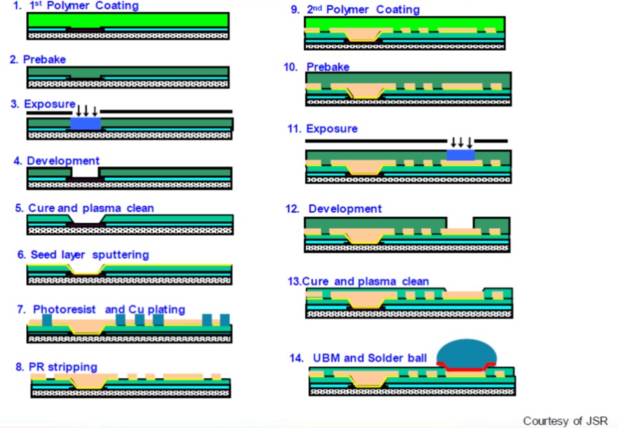
Figure 2. Process for application of the photosensitive dielectric materials (RDL1 and RDL2)

Since the RDL will be placed on the surface of the reconstituted circular wafer, the RDL dielectric solution (with solvent) is typically spin coated onto the surface as shown in step 1.  The solvent is then removed during the prebake.  Step 3 is to expose through a suitable mask for form the desired circuit lines and vias.  The process in Figure 2 is for a positive tone photoresist, so the exposure renders the irradiated material less soluble in step 3.  The exposed areas are removed using a developer solution in step 4.  The remaining dielectric is cured at the specific temperature dictated by the polymer type used for the dielectric.  The cured dielectric is then cleaned using a plasma to remove any unwanted polymer in step 5.  Step 6 involves the sputtering of a seed layer via in the areas where copper needs to be plated.  A traditional photoresist is used to pattern the lines and vias.  Step 7 shows the combination of the photoresist application, exposure, develop and copper plating.  After the copper traces and vias are formed, the resist is stripped (removed) and the desired copper lines and vias are completely formed.  Steps 9-13 are used to form the second dielectric layer (RDL2).  The final step in the process is to plate the under bump metallurgy (UBM) and place and reflow the solder balls.

In the next post we will discuss in greater detail the polybenzoxazole (PBO) materials used for the redistribution layers.

Share on LinkedIn Share

Filed Under: Uncategorized

« Polymers in Electronics Part Five: Redistribution Layers for Fan-Out Wafer Level Packaging
Polymers in Electronics Part Seven: Redistribution Layers for Fan-Out Wafer Level Packaging »

Comments

  1. Tarhib IT Limited says

    June 25, 2024 at 3:02 AM

    Very insightful breakdown of redistribution layers in wafer-level packaging! Understanding these details is crucial for anyone interested in polymer electronics. Thanks for sharing!

Leave a Reply

Your email address will not be published. Required fields are marked *

Polymer Innovation Blog

I’m Dr. Jeff Gotro and welcome to the Polymer Innovation Blog. Over the last 40 years I have been involved in polymer research, along with product and process development. I acquired invaluable experience working for IBM, AlliedSignal, Honeywell, Ablestik Labs (now Henkel) and in multiple consulting projects. In this blog, I (along with some guest contributors) will share our experiences, tips, and “tricks of the trade” to get more out of your innovation efforts and discuss new trends and technical advances in the polymer industry.
View Jeff Gotro, Ph.D., CMC's profile on LinkedIn

Innocentrix, LLC


Click to Visit Website

plastics expert witness
Click for More Information

Subscribe by Email

Search the Blog

Polymer Video Training

Visit our Video Store

Polymers in Electronic Packaging

polymers in electronic packaging Are you confused about what is electronic packaging? Have you ever wondered what type of polymers and polymer-based composites are used in electronics? Learn More...

Practical Tips for Curing Thermosets

practical tips for curing thermosets Have you ever had a question about the degree of cure or is your part fully cured after processing? Confused about what is gelation or how does vitrification impact thermoset curing? Learn More...

Rheology of Thermosets

rheology of thermosets Have you ever had a question about measuring the rheological properties of thermosets Didn’t know what is the right experimental approach to get the right rheological information? Learn More...

Dielectric Cure Monitoring of Thermosets

Dielectric Cure Monitoring of Thermosets Do you have a need for an in-situ cure monitor for a thermoset process but don’t know where to start? Are you confused about the terminology used in dielectric spectroscopy? Learn More...

Introduction to Biopolymers and Bioplastics

Introduction to Biopolymers and Bioplastics Would you like to know how sustainable are bio-based polymers? Or what is the market size and growth rate for bioplastics? Or have questions about the biomass supply chain? Learn More...

Thermoset Characterization

Thermoset Characterization Have you ever had a question about how to measure a physical property of a thermoset? Confused about what is gelation or how does vitrification impact thermoset curing profiles? Or wondered how to measure the glass transition temperature of an epoxy or polyester composite? Learn More...

Amazon.com Bookshelf

Robert's Rules of Innovation Thermal Analysis of Polymers Order

Copyright © 2025 Innocentrix, LLC · All Rights Reserved