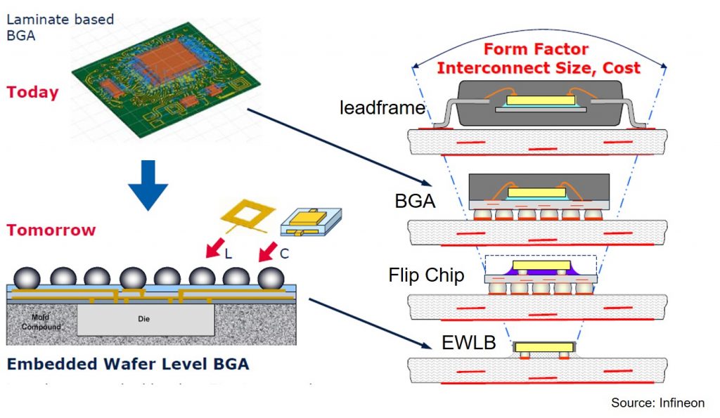
If you take the cover off your desktop PC (If you have one and I don’t recommend trying this on your laptop or phone!) you will see many components soldered to a printed circuit board (motherboard). Many of these surface mounted devices are packaged semiconductor chips. In electronics, the term packaging refers to the technologies used to route the electrical signals from the chip to other components in the device. Packaging typically includes many polymers in the form of circuitized substrates, protective coatings on the substrates (soldermask), encapsulants such as mold compounds and underfills (under a flip chip). In Figure 1 below, the top left image shows a printed circuit board with multiple components attached to the top surface. The right side of Figure 1 shows the technology progression from leadframe packages to ball grid array (BGA) packages to flip chip packages to embedded wafer level BGA (eWLB). All of these packages use a mold compound to encapsulate and protect the semiconductor chip as seen in the gray area in the leadframe and BGA. The purple material under the chip in the Flip chip package is called an underfill and is used to stabilize the metal used for chip interconnect (either a solder ball as shown in Figure 1 or some of the higher density flip chips use copper pillars).
Figure 1. Technology progression towards wafer level packaging
In this post we will discuss the typical mold compounds used in leadframe, BGA, and flip chip packaging. In subsequent posts we will discuss the specialized mold compound required for eWLB.
Epoxy mold compounds (EMC) are highly formulated products that contain epoxy resins, curing agents, accelerators, fillers, flame retardants, adhesion promoters, parting agents (allows release from the mold wall after molding), pigments like carbon black and other proprietary additives. Each EMC supplier has their formulation “tricks” to tailor the properties to the application and molding process (1).
The epoxy resin most commonly used in EMC is epoxy cresol novolac resins cured with phenolic curing agents.
EMC’s are typically highly filled using spherical silica to reduce the coefficient of thermal expansion. The first generation mold compounds have the following advantages:
- Ease of processing with good mold filling, low wire sweep
- Good adhesion to leadframes, packaging substrates, and semiconductor dies
- Acceptable chemical and moisture resistance
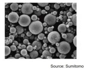
The spherical silica fillers usually have a multimodal particle size distribution to allow for high filler loadings (2). High filler loadings increase the viscosity of the uncured resins which could have detrimental effects during the molding process. The spherical shape helps to keep the viscosity manageable during mold filling (think about round marbles rolling past one another during flow). The SEM image below shows spherical fillers used in epoxy mold compound formulations. In the SEM image it is easy to see how the small and medium sized filler particles will “nest” in the spaces between the larger spheres.
Some EMC’s contain biphenyl epoxy resins to improve the following properties:
- Enable low viscosity for wire sweep control during molding
- Allow for higher filler loading (added advantage from the lower resin viscosity)
- Lowers moisture absorption which improve the package reliability
In the next post we will discuss the EMC molding and curing process.
References
1) S. Komori and Y Sakamoto, Materials for Advanced Packaging, Chapter 10, D. Lu and CP Wong, Editors, Springer, 2009
2) https://polymerinnovationblog.com/fillers-action-achieve-high-particle-loadings-part-two/


I worked on this at MCC and SEMATECH. 1984-1992.