Source: Yole Developpement
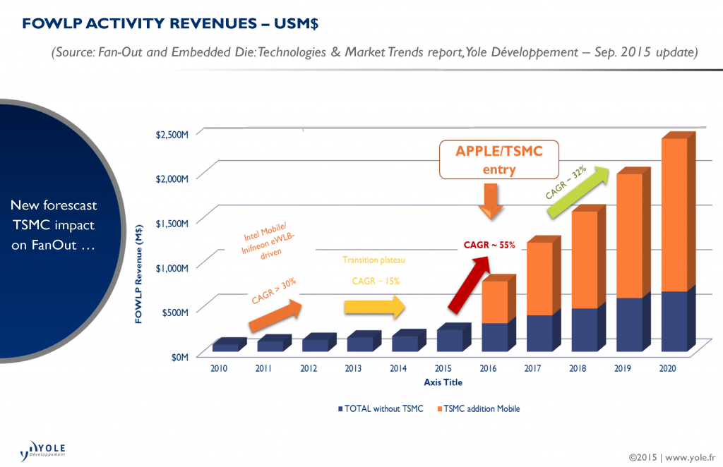
I attended the International Microelectronics Assembly and Packaging Society (IMAPS) Device Packaging Conference held in Scottsdale, AZ the week of March 6, 2017. The major theme of the technical sessions was the emergence of Fan-Out Wafer Level packaging in multiple applications. The most prominent application driving the market was the TSMC InFO process to package the Apple iPhone 7 A10 processor. As seen in the graph above, when Apple and Taiwan Semiconductor Manufacturing Corporation (TSMC) partnered to use the integrated fan-out (InFO) wafer level type package, the growth rate accelerated dramatically. The TSMC InFO package is described in US Patent 9,000,584. The interesting feature is the blue bars represent the entire rest of the market applications. With Apple/TSMC driving the market, the FOWLP revenues are projected to reach $2.5 billion in 2020.
There are many variations of fan-out wafer level packaging offered by various OSATS and foundries. There are three main types of FOWLP:
- Chip first, die face down
- Chip first, die face up
- Chip last, die face down (essentially a flip-chip on a known good polymer redistribution layer)
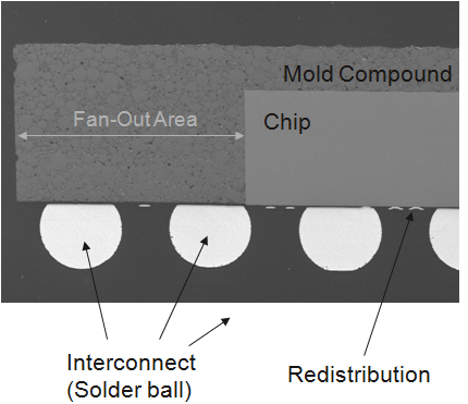
In all of these types of applications, polymers play a key role in the electronic packaging. In the image below, epoxy mold compound is used to encapsulate the chip and provide a planar surface for the fan-out of the redistribution layer.
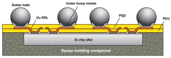
The epoxy mold compound is highly filled to lower the CTE and to control shrinkage. We will discuss mold compounds used in fan-out wager level packaging in the next several posts. Various polymers such as photosensitive polyimides, polybenzoxazole (PBO), and polybenzocyclobutane (BCB) have been developed for use as dielectric redistribution layers. The redistribution layers are in yellow in the figure below. The schematic below is an example of the chip first, die face down. It’s a bit complicated, but we will make things clear in our subsequent posts. The epoxy molding compound provides the surface to enable the placement of the redistribution layers allowing the copper redistribution (Cu RDL) to “fan-out” away from the center of the chip (die). For reliability (such as drop testing) good adhesion is required between the polymer dielectric and the mold compound.
Source: HD MicroSystems
Recently, the curing temperatures for PBO and BCB’s have been lowered to enable better process compatibility with the epoxy mold compound. Additionally, these materials are required to be photopatterned to allow connections from PI (1) to PI (2).
In the next series of posts, we will provide a more detailed discussion on recent advances in polymers used in fan-out wafer level packaging.


Leave a Reply