

I was on vacation last week and on the plane back to Orange County, I watched the movie "Hidden Figures" the story of the black female "computers" at NASA Langley in the early days of the space program. First of all, it was a great movie and a true story. Secondly, I was surprised I didn't know about the history of the legendary African American female computers. During the ... [Click to Continue...]
Polymers in Electronics Part Seven: Redistribution Layers for Fan-Out Wafer Level Packaging
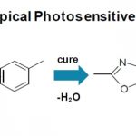
This post will describe the use of a photosensitive positive-tone dielectric based on polybenzoxazole (PBO) used as the redistribution layers (RDL) in Fan-Out Wafer Level Packaging (FOWLP). To meet the challenges for FOWLP, such as lower curing temperatures (compared with polyimides that cure at over 300°C), low modulus, high elongation, and good electrical insulation, HD ... [Click to Continue...]
Polymers in Electronics Part Six: Redistribution Layers for Fan-Out Wafer Level Packaging
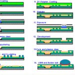
The last post introduced the use of a polymer dielectric as a redistribution layer (RDL) as a means to fan-out circuit traces from the chip to the backside of the package. In the image on the left, the RDL layers are shown in green (RDL1) and purple (RDL2). The RDL layers (also called dielectric layers) are applied to the reconstituted wafer and imaged using photolighography. ... [Click to Continue...]
Polymers in Electronics Part Five: Redistribution Layers for Fan-Out Wafer Level Packaging
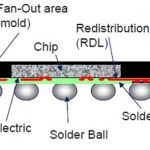
The last post focused on molding compounds used in Fan-Out Wafer Level Packaging (FOWLP) as seen in black in the image above (source Infineon). A key enabler in the fan-out package is the polymer redistribution layer (RDL) or sometimes referred to as the dielectric layer. There are several types of polymers used as photosensitive dielectrics in FOWLP: Polyimide (PI) ... [Click to Continue...]
Polymers in Electronic Packaging Part Four: Molding Process for Epoxy Mold Compounds for Fan-Out Wafer Level Packaging
This post will focus on the epoxy molding process using liquid and solid EMC for FOWLP. In the image on the left, a liquid EMC is shown on the surface of the partially reconstituted wafer prior to compression molding (source: Nanium). For FOWLP, the compression molding process is different compared with the transfer molding process typically used for EMC’s. A schematic of ... [Click to Continue...]