
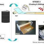
Figure 1. Build-up material roadmap (source: Ajinomoto Fine-Techno Co. Inc.) The last post described the chemistry and types of build-up films typically used in the electronic packaging industry. We also touched on the build-up material roadmap which showed the various complex packaging substrates that are enabled using build-up film technology as shown in Figure 1. ... [Click to Continue...]
Polymers in Electronic Packaging: Build-Up Films for Flip Chip Semiconductor Substrates, Part Two
Figure 1. Cross section of a 1+4+1 HDI substrate using Ajinomoto build-up film (ABF) The previous post discussed the geometry of the ABF products and the process used to build-up the circuit layers on the core. In Figure 1 above, there is one layer of ABF on each side of the 4 layer BT epoxy core. Notice in this schematic construction the plated through holes (PTH) extend ... [Click to Continue...]
Polymers in Electronic Packaging: Build-Up Films for Flip Chip Semiconductor Substrates, Part One
Figure 1. An example of a HDI substrate used for a Flip Chip BGA (source: NXP Freescale) The last post described High Density Interconnect (HDI) substrates. This post will discuss the build-up layer technologies used to make the sequential circuit layers on each side of the BT epoxy core. In Figure 1, a cross-section of a 4+2+4 HDI substrate is shown. There are 4 ... [Click to Continue...]
Polymers in Electronic Packaging: Semiconductor Substrates for Flip Chip
Figure 1. Cross section of FC-BGA multilayer semiconductor HDI substrate The driving force for adoption of flip-chip packaging was the rapidly increasing bump count on logic chips thus requiring a higher routing density semiconductor substrate. The wire bond PBGA typically utilized a two sided BT substrate which provided adequate fan-out and communication with the ... [Click to Continue...]
Polymers in Electronic Packaging: Introduction to Semiconductor Substrates
Figure 1. Cross section of PBGA package showing a multilayer semiconductor substrate (Source: NXP Freescale) A previous post described the plastic ball grid array (PBGA) package. This post will provide an introduction to semiconductor substrate technology. In Figure 1, the semiconductor substrate is directly under the wire-bonded silicon die. In many PBGA’s with ... [Click to Continue...]