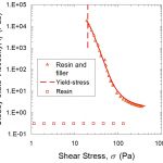
This post will cover the interpretation of a typical controlled stress flow curve for a highly filled uncured material. In many electronic applications, the adhesive or coating is applied to the substrate using dispensing equipment where the filled material is in a syringe and either air pressure or an auger is used to flow the material through a small needle onto the ... [Click to Continue...]
Polymers in Electronic Packaging: Rheological Measurements, Part 3
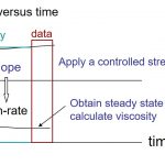
Rheometers are used to determine the viscosity by measuring the stress at a known shear-rate or measuring the shear rate at a known stress. There are two types of torsional rheometers: Controlled strain (most common) Controlled stress In the case of the strain controlled rotational rheometer, a typical configuration is shown in the following figure: In this ... [Click to Continue...]
Polymers in Electronic Packaging: Rheological Measurements
The rheological properties of polymers used in electronic packaging applications spans a wide range of fluid types and viscosity ranges. In the uncured state, many adhesives, coatings, mold compounds, and underfills have interesting rheological behavior. Many of these types of materials are highly filled to achieve the desired mechanical properties such as low coefficient of ... [Click to Continue...]
Happy Memorial Day
Have a safe and relaxing Memorial Day. I'm at ECTC this week so I will be back with our continuing series on Polymers in Electronic Packaging next Monday. Thanks to all of my loyal readers, we topped 1900 visitors per week in May! ... [Click to Continue...]
Polymers in Electronic Packaging: Introduction to Rheology
I will start this post with a short personal story about how I got into electronic packaging and specifically, rheology in electronic packaging. When I was a fourth year graduate student at Northwestern I started looking for a job at the typical places an industrial polymer rheologist might consider, like Dow, DuPont, GE Plastics and others. My thesis advisor, Prof. William ... [Click to Continue...]


